

IGBT or like semiconductor device of high voltage-withstanding capability
- Summary
- Abstract
- Description
- Claims
- Application Information
AI Technical Summary
Benefits of technology
Problems solved by technology
Method used
Image

Examples
embodiment
of FIG. 3
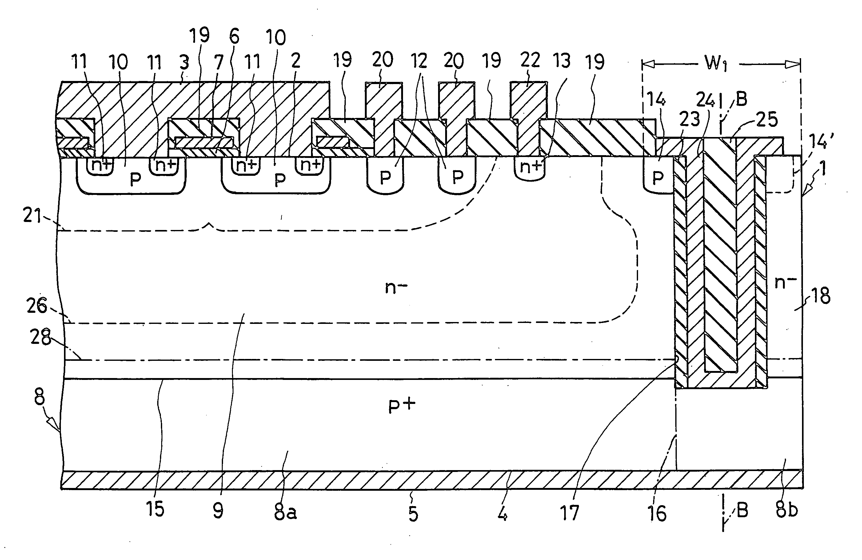
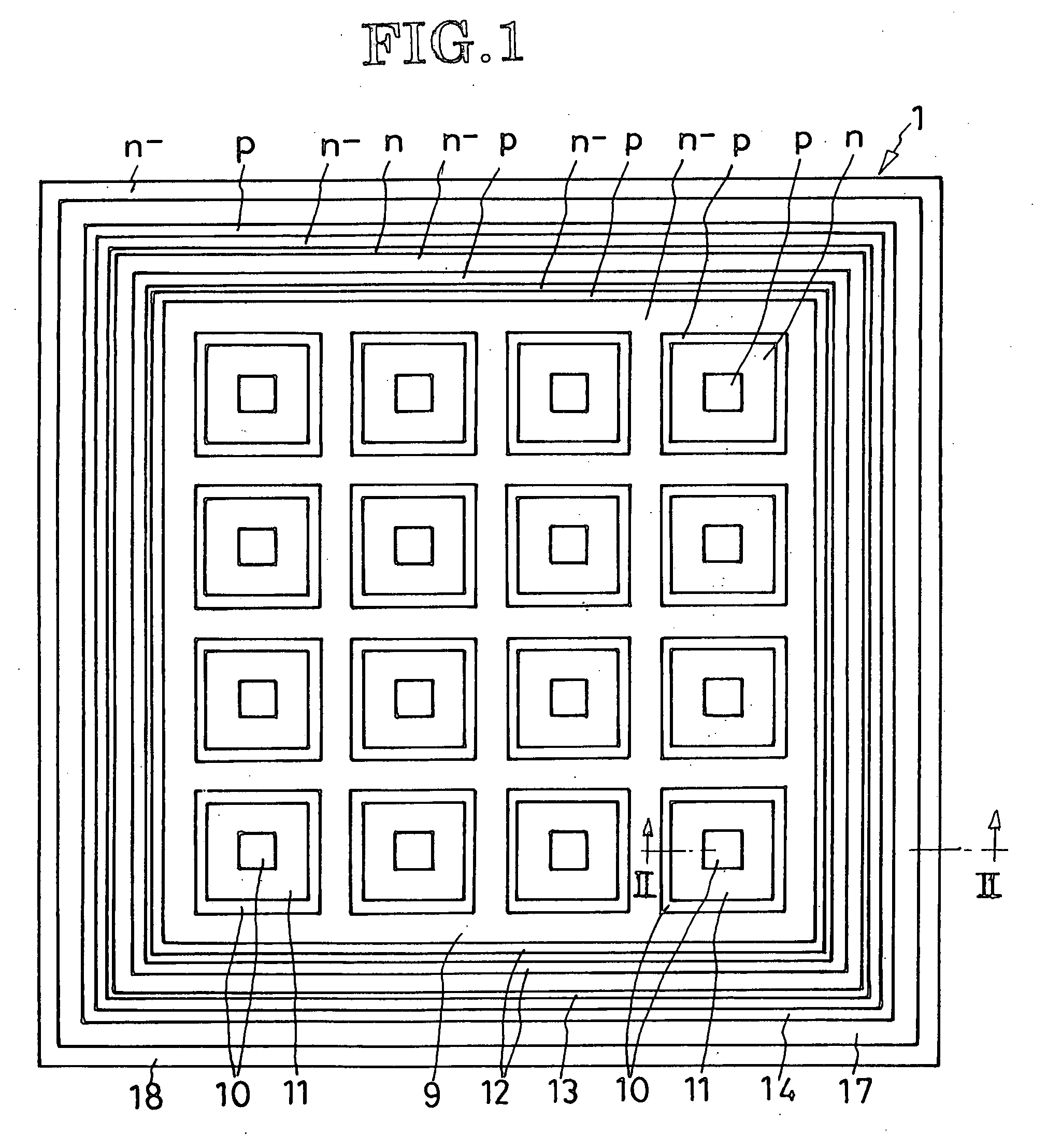
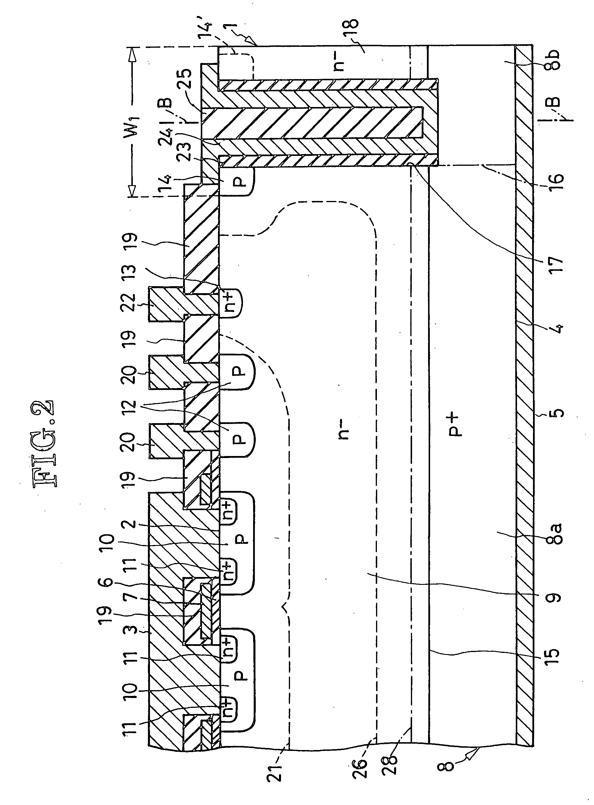
[0068] The second preferred form of multiple-cell IGBT chip shown in FIG. 3 features an additional set of, four in this embodiment, p-type reverse guard rings 27, all the other details of construction being as previously set forth in connection with FIGS. 1 and 2. The additional reverse guard rings 27 extend from the first major surface 2 of the substrate 1 down into the substrate base region 9 to relatively shallow depths. Disposed concentrically between the channel limiter ring 13 and the preexisting reverse guard ring 14, the additional reverse guard rings 27 thoroughly encircle the array of IGBT cells comprised of the islandlike cell base regions 10 and annular emitter regions 11.
[0069] As will be understood from a closer examination of FIG. 3, the additional reverse guard rings 27 have progressively greater spacings from one to the next as they approach the channel limiter ring 13. Further the inmost additional reverse guard ring 27, placed closest to the channel limi...
PUM
 Abstract
Description
Claims
Application Information