Method of fabricating a thin-film solar cell, and thin-film solar cell

Inactive Publication Date: 2006-11-30
SHARP KK
View PDF2 Cites 50 Cited by
  • Summary
  • Abstract
  • Description
  • Claims
  • Application Information

AI Technical Summary

Benefits of technology

[0009] If the trimming method with a conventional laser scribing method is adopted, however, a portion of the transparent electrode layer volatilized by the irradiation of the fundamental harmonic of the YAG laser light adheres on a vertical cross section of the

Problems solved by technology

This forms a leak path between the transparent electrode layer and the back surface electrode layer, and the

Method used


Image

  • Method of fabricating a thin-film solar cell, and thin-film solar cell
  • Method of fabricating a thin-film solar cell, and thin-film solar cell
  • Method of fabricating a thin-film solar cell, and thin-film solar cell

Examples


first example

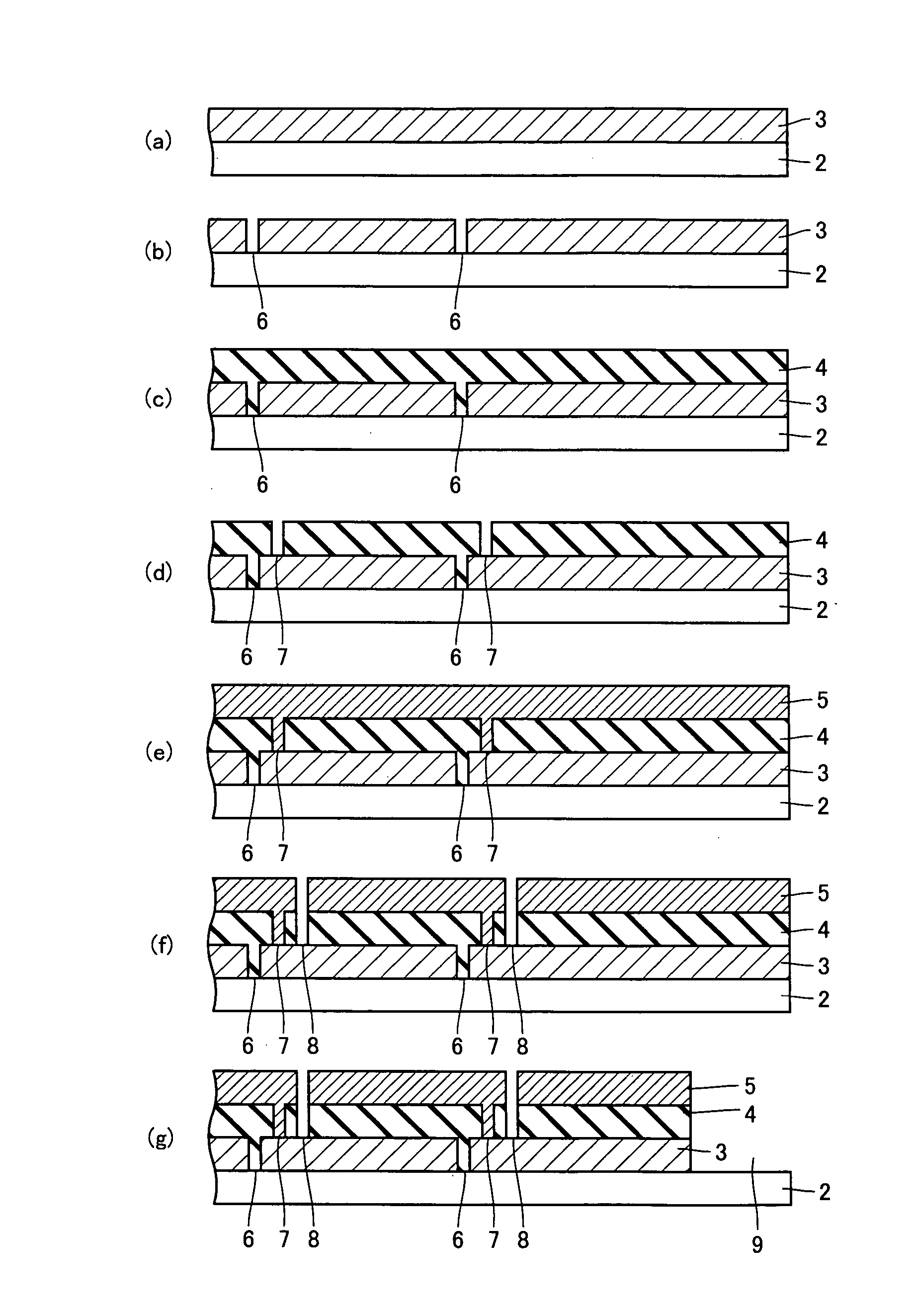
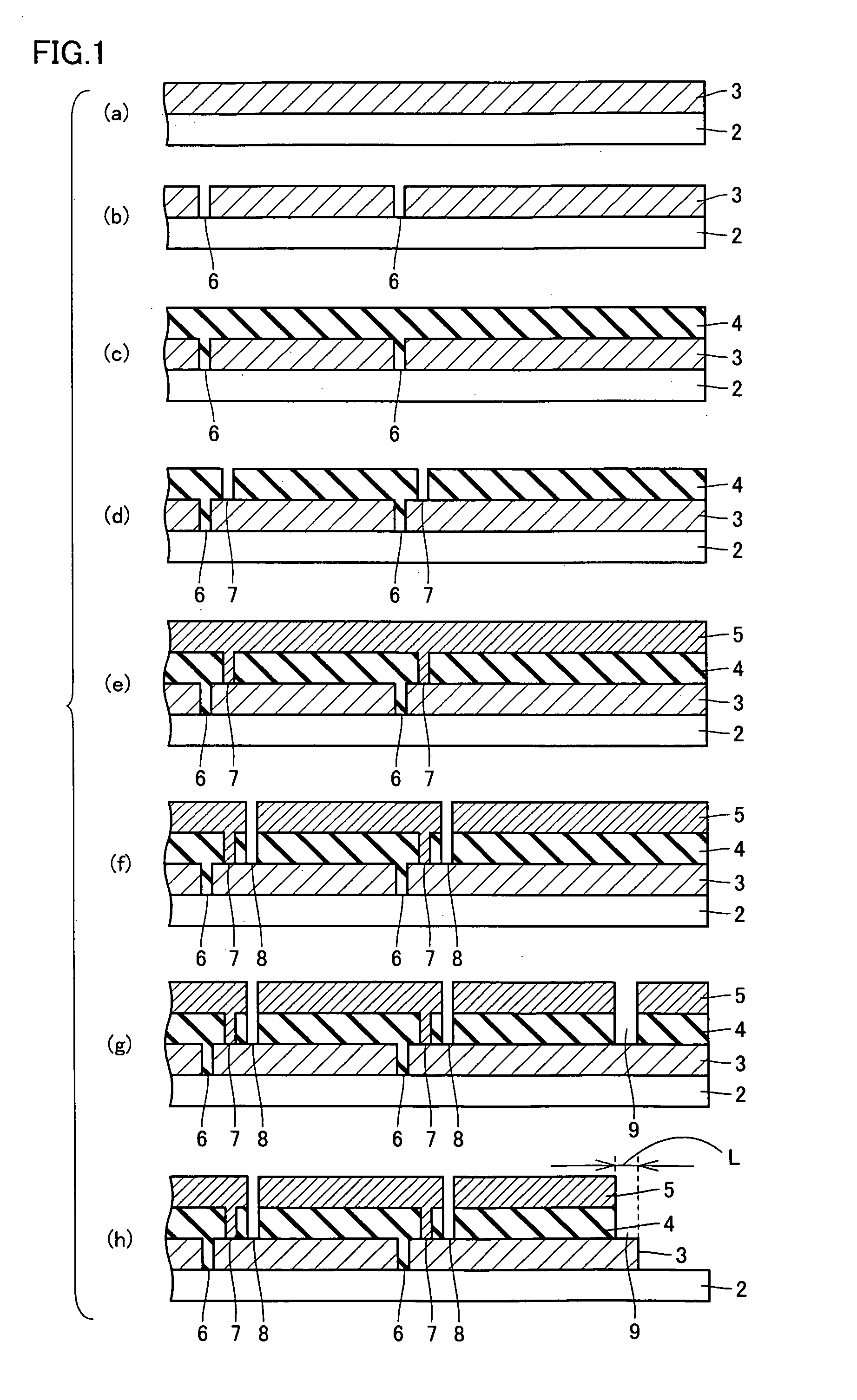
[0039] Initially, as shown in FIG. 1(a), there was prepared transparent insulator substrate 2 implemented by a glass substrate having a surface in the form of a rectangle having a width of 560 mm by a length of 925 mm and having transparent conductive layer 3 formed of SnO2 deposited thereon.

[0040] Then, a fundamental harmonic of YAG laser light was irradiated from a side of transparent insulator substrate 2 to laser-scribe and thus remove a portion of transparent conductive layer 3 in a strip to form, as shown in FIG. 1(b), 50 first isolation grooves 6 of 0.1 mm in width in the longitudinal direction of transparent insulator substrate 2 such that adjacent first isolation grooves 6 had equal intervals therebetween. Transparent insulator substrate 2 was then cleaned with pure water ultrasonically.

[0041] Then, plasma CVD was employed to deposit a p layer formed of a boron-doped, hydrogenated amorphous silicon-based semiconductor (a-Si: H), then an i layer formed of an undoped, hydro...


PUM


Abstract

There is provided a method of fabricating a thin-film solar cell including the steps of: irradiating a first laser light from a side of the substrate to remove the semiconductor and back surface electrode layers; and irradiating a second laser light from the side of the substrate to remove the transparent electrode, semiconductor and back surface electrode layers at a region outer than the region irradiated with the first laser light. There is provided a thin-film solar cell including a transparent electrode layer, a photoelectric conversion semiconductor layer and a back surface electrode layer deposited on a transparent insulator substrate in this order, wherein the solar cell has a perimeter with the transparent electrode layer protruding outer than the semiconductor and back surface electrode layers.

Description

[0001] This nonprovisional application is based on Japanese Patent Application No. 2005-155980 filed with the Japan Patent Office on May 27, 2005, the entire contents of which are hereby incorporated by reference. BACKGROUND OF THE INVENTION [0002] 1. Field of the Invention [0003] The present invention relates to methods of fabricating thin-film solar cell, and such thin-film solar cell, and particularly to methods of fabricating thin-film solar cell capable of reducing a leak current at a perimeter thereof, and such thin-film solar cell. [0004] 2. Description of the Background Art [0005] Various types of solar cell converting the energy of sunlight directly to electrical energy have been practically used. Among others, a thin-film solar cell that employs thin amorphous silicon film is actively being developed as it is readily processed at low temperature and increased in area to have a large area and can hence be fabricated inexpensively. [0006]FIG. 2 is a schematic cross section o...

Claims


Application Information

Patent Timeline
IPC IPC(8): H01L31/00
CPCH01L31/022425H01L31/046Y02E10/50H01L31/0463
Inventor TAKEDA, TORUTACHIBANA, SHINSUKE
Owner SHARP KK
Why Eureka
Try Eureka