Pulsed plasma deposition for forming microcrystalline silicon layer for solar applications

a microcrystalline silicon and solar cell technology, applied in the field of solar cells, can solve the problems of reducing the conversion efficiency of pv solar cells, reducing the manufacturing throughput, and increasing production costs

Inactive Publication Date: 2010-10-14
APPLIED MATERIALS INC
View PDF3 Cites 20 Cited by
  • Summary
  • Abstract
  • Description
  • Claims
  • Application Information

AI Technical Summary

Problems solved by technology

However, a production worthy process has yet to be developed to be able to provide PV devices at high deposition rate and high film quality as well as low manufacturing cost.
For example, insufficient crystallinity of the silicon film may cause incomplete formation and fraction

Method used


Image

  • Pulsed plasma deposition for forming microcrystalline silicon layer for solar applications
  • Pulsed plasma deposition for forming microcrystalline silicon layer for solar applications
  • Pulsed plasma deposition for forming microcrystalline silicon layer for solar applications

Examples


Embodiment Construction

[0019]The present invention describes a method to deposit an intrinsic type microcrystalline silicon layer with high deposition rate, high and uniform crystalline fraction, and low manufacturing cost. In one embodiment, the intrinsic type microcrystalline silicon layer may be deposited by a plasma process having a first deposition mode and a second deposition to form an intrinsic type microcrystalline silicon seed layer and a bulk intrinsic type microcrystalline silicon layer respectively. In one embodiment, the intrinsic type microcrystalline silicon layer may be used in a multi-junction solar cell or a single junction solar cell.

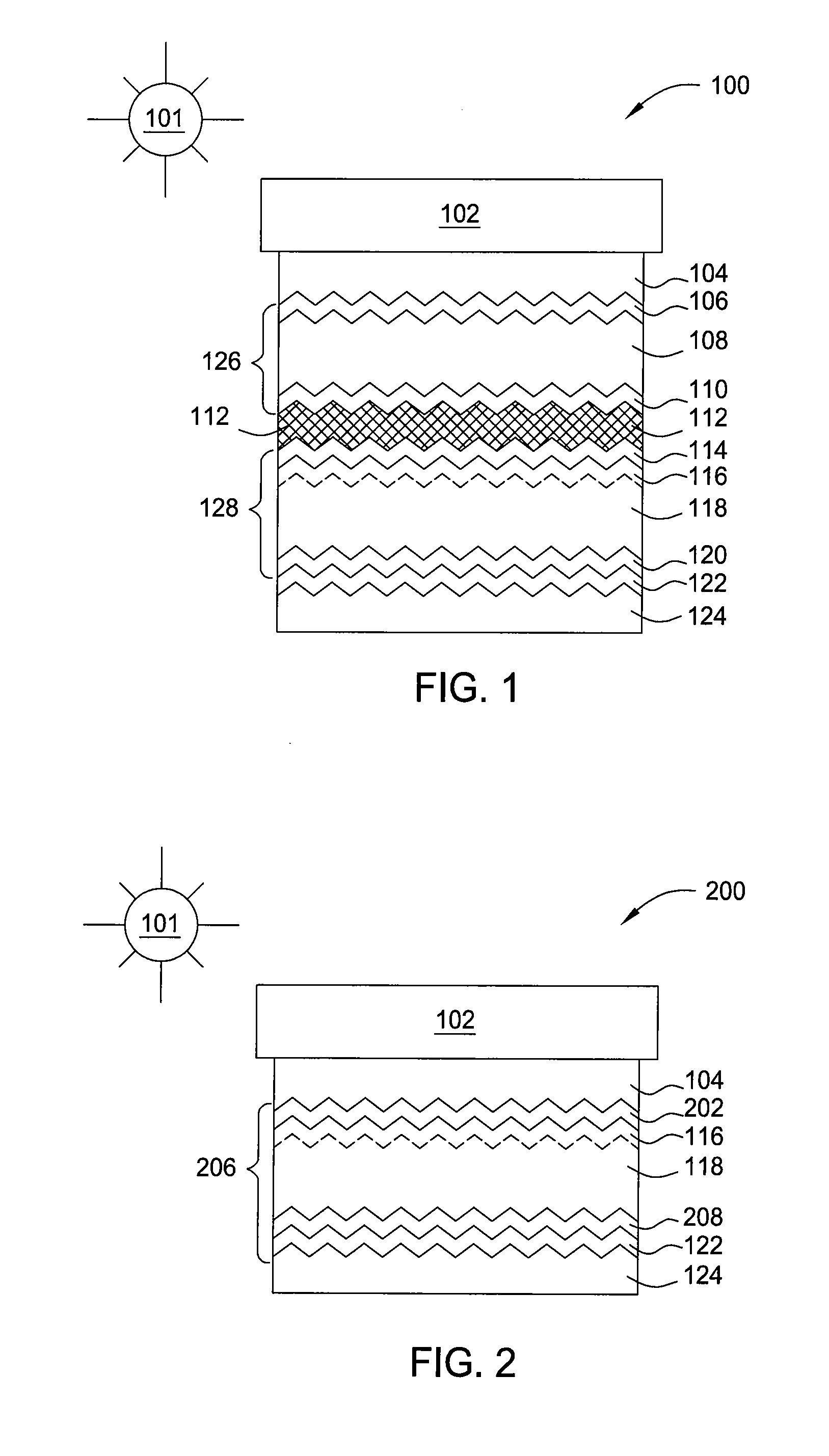
[0020]FIG. 1 is a schematic diagram of an embodiment of a multi-junction solar cell 100 oriented toward the light or solar radiation 101. Solar cell 100 comprises a substrate 102, such as a glass substrate, polymer substrate, metal substrate, or other suitable substrate, with thin films formed thereover. The solar cell 100 further comprises a first transpa...


PUM

PropertyMeasurementUnit
Timeaaaaaaaaaa
Timeaaaaaaaaaa
Timeaaaaaaaaaa

Abstract

A method for an intrinsic type microcrystalline silicon layer is provided. In one embodiment, the microcrystalline silicon layer is fabricated by providing a substrate into a processing chamber, supplying a gas mixture into the processing chamber, applying a RF power at a first mode in the gas mixture, pulsing the gas mixture into the processing chamber, and applying the RF power at a second mode in the pulsed gas mixture.

Description

BACKGROUND OF THE INVENTION[0001]1. Field of the Invention[0002]Embodiments of the present invention generally relate to solar cells and methods for forming the same. More particularly, embodiments of the present invention relate to a method of forming a microcrystalline silicon layer utilized in solar applications.[0003]2. Description of the Related Art[0004]Photovoltaic devices (PV) or solar cells are devices which convert sunlight into direct current (DC) electrical power. PV or solar cells typically have one or more p-n junctions. Each junction comprises two different regions within a semiconductor material where one side is denoted as the p-type region and the other as the n-type region. When the p-n junction of the PV cell is exposed to sunlight (consisting of energy from photons), the sunlight is directly converted to electricity through the PV effect. PV solar cells generate a specific amount of electric power and cells are tiled into modules sized to deliver the desired amo...

Claims


Application Information

Patent Timeline
IPC IPC(8): H01L31/00H01L21/20
CPCH01L21/02532H01L21/02576H01L21/02579H01L21/02595Y02E10/548H01L31/076H01L31/077H01L31/1824Y02E10/545H01L21/0262Y02E10/547Y02P70/50
Inventor SHENG, SHURANCHAE, YONG KEE
Owner APPLIED MATERIALS INC
Why Eureka
Try Eureka