
Cell based integrated circuit and unit cell architecture therefor

Inactive Publication Date: 2002-06-04
LAPIS SEMICON CO LTD
View PDF6 Cites 114 Cited by
  • Summary
  • Abstract
  • Description
  • Claims
  • Application Information

AI Technical Summary

Benefits of technology

Accordingly, an object of the present invention is to provide a method for designing a unit cell that contributes for increasing the degree of integration of the integrated circuit.
Another object of the present invention is to provide a unit cell that contributes for increasing the degree of integration of the integrated circuit.
Further object of the present invention is to provide an integrated circuit of which the degree of integration can be increased.

Problems solved by technology

According to the conventional unit cell, power line (Vdd) and ground line (Vss) across the P-type active region and N-type active region; therefore the arrangement of conductive lines becomes complicated.
As a result, it becomes difficult to increase the degree of integration of the IC.
Further, conductive lines connecting the poly-silicon lines on the P-type active region and N-type active regions may across the signal lines, therefore the arrangement of conductive lines becomes complicated.
As a result, it becomes difficult to increase the degree of integration of the IC.

Method used


Image

  • Cell based integrated circuit and unit cell architecture therefor
  • Cell based integrated circuit and unit cell architecture therefor
  • Cell based integrated circuit and unit cell architecture therefor

Examples


Embodiment Construction

In the following detailed description of the preferred embodiments, reference is made to the accompanying drawings which form a part hereof, and in which is shown by way of illustration specific preferred embodiments in which the inventions may be practiced. These embodiments are described in sufficient detail to enable those skilled in the art to practice the invention, and it is to be understood that other embodiments may be utilized and that logical, mechanical and electrical changes may be made without departing from the spirit and scope of the present inventions. The following detailed description is, therefore, not to be taken in a limiting sense, and scope of the present inventions is defined only by the appended claims.

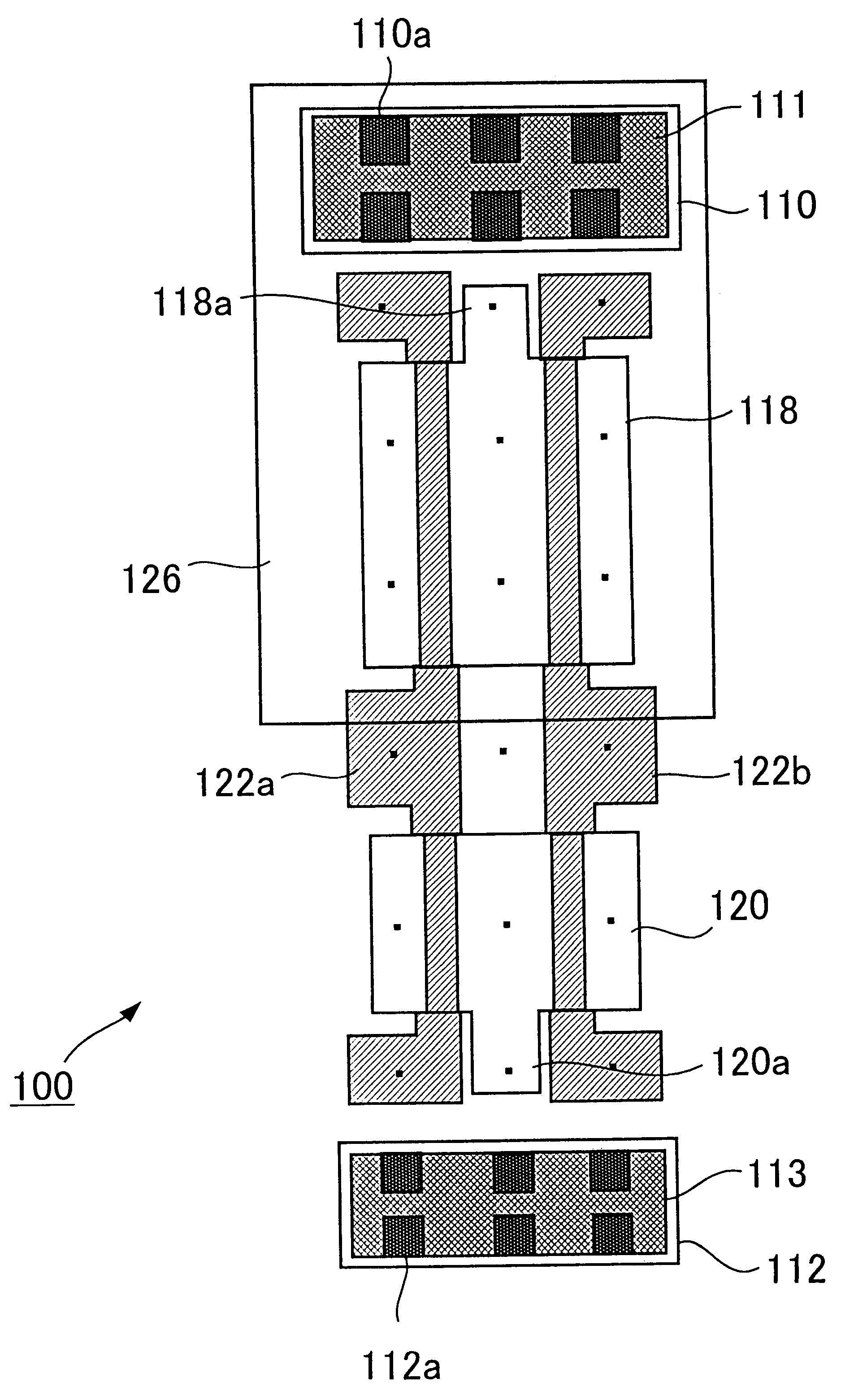
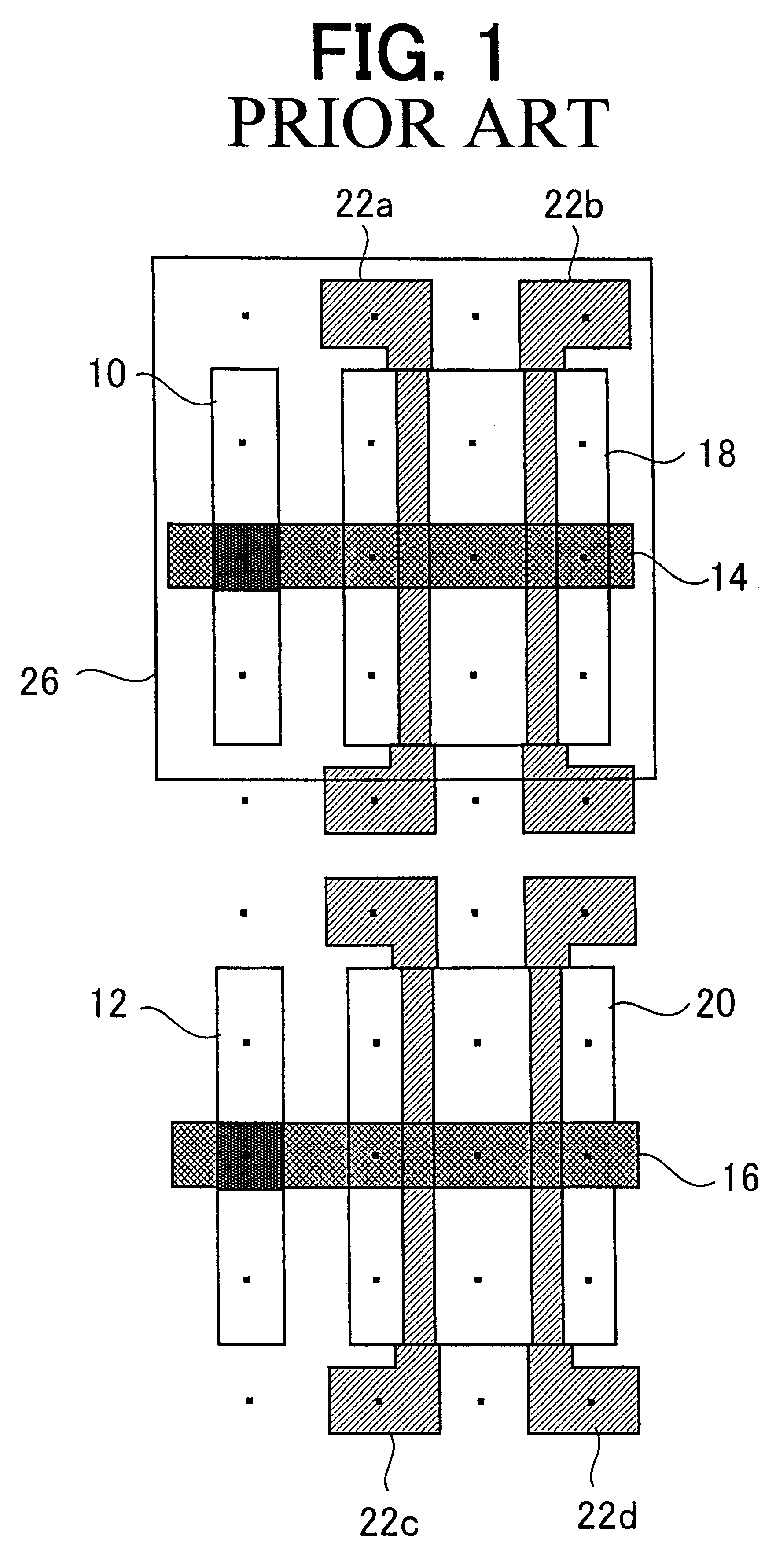
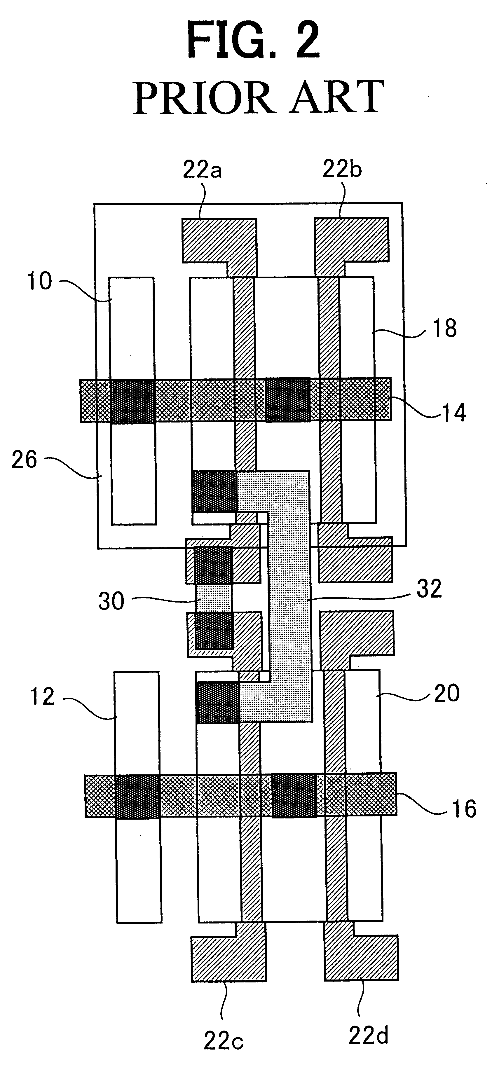
For better understanding of the present invention, a conventional technology is first described. FIG. 1 shows a conventional unit cell architecture. The unit cell includes an N-type well contact region 10 (N+ contact region) for Vdd (distributed power); a subs...


PUM


Abstract

In a unit cell, a first conductive type active region and a second conductive type active region are provided. Those two active regions extend in a first direction. Each of the active regions have first and second ends thereof. The first end of the second conductive type active region opposes the second end of the first conductive type active region. A conductive pattern is provided to extend in the first direction across the first conductive type active region and the second conductive type active region. A first contact region is arranged adjacent the first end of the first conductive type active region in the first direction. A second contact region is arranged adjacent the second end of the second conductive type active region in the first direction.

Description

The present invention relates to cell based integrated circuits and unit cell architecture for such circuits, which result in significant improvement of the degree of integration.Cell based integrated circuit technology and cell architecture for such circuits have been developed as quick-turns integrated circuit (IC) design methodologies in which pre-designed circuit units or cells are wired together to rapidly implement a new IC functionality. The pre-designed circuit elements are called macro cells which are made by interconnecting unit cells.A conventional unit cell includes a P-type active region (PMOS transistor) and an N-type active region (NMOS transistor), which are arranged in a first direction. A pair of poly-silicon regions is formed on each of the P-type and N-type active regions. Those poly-silicon regions are extending in parallel to each other in the first direction. The unit cell also includes first and. second substrate contact regions, which are arranged in paralle...

Claims


Application Information

Patent Timeline
IPC IPC(8): H01L21/02H01L21/70H01L21/336H01L21/8238H01L27/10G06F17/50H01L27/02H01L27/118
CPCH01L27/11807H01L27/0207
Inventor MASUDA, HIROHISAISHIKAWA, HIROKAZU
Owner LAPIS SEMICON CO LTD
Features
  • Generate Ideas
  • Intellectual Property
  • Life Sciences
  • Materials
  • Tech Scout
  • Unparalleled Data Quality
  • Higher Quality Content
  • 60% Fewer Hallucinations
Learn More