System for controlling transistor spacer width

a technology of spacer width and transistor, which is applied in the direction of transistor, semiconductor/solid-state device testing/measurement, coating, etc., can solve the problems of reducing revenue, widening the speed distribution of devices produced, and not always constant final width of spacers formed

Inactive Publication Date: 2002-06-25
GLOBALFOUNDRIES INC
View PDF13 Cites 22 Cited by
  • Summary
  • Abstract
  • Description
  • Claims
  • Application Information

AI Technical Summary

Problems solved by technology

Due to variations in the initial thickness of the insulative layer, the conformality of the insulative layer, and the accuracy of the endpointing process, the final width of the spacers formed is not always constant.
Lack of effective spacer width control widens the speed distributions of the devices produced.
Faster devices have a higher market value; hence, wider speed variations equate to reduced revenue.

Method used


Image

  • System for controlling transistor spacer width
  • System for controlling transistor spacer width
  • System for controlling transistor spacer width

Examples


Embodiment Construction

Illustrative embodiments of the invention are described below. In the interest of clarity, not all features of an actual implementation are described in this specification. It will of course be appreciated that in the development of any such actual embodiment, numerous implementation-specific decisions must be made to achieve the developers' specific goals, such as compliance with system-related and business-related constraints, which will vary from one implementation to another. Moreover, it will be appreciated that such a development effort might be complex and time-consuming, but would nevertheless be a routine undertaking for those of ordinary skill in the art having the benefit of this disclosure.

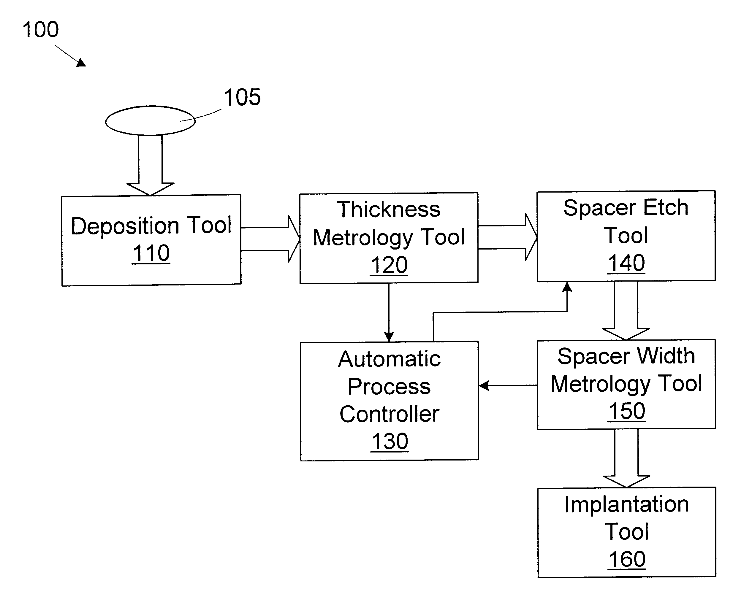
Referring now to the Figures, and particularly to FIG. 1, a simplified block diagram of a processing line 100 useful for forming spacers a semiconductor device is provided. The processing line processes a plurality of wafers 105, either in lots or individually. The operation of the pro...


PUM

PropertyMeasurementUnit
thickness metrologyaaaaaaaaaa
thicknessaaaaaaaaaa
widthaaaaaaaaaa

Abstract

A method for controlling spacer width in a semiconductor device is provided. A substrate having a gate formed thereon is provided. An insulative layer is formed over at least a portion of the substrate. The insulative layer covers the gate. The thickness of the insulative layer is measured. A portion of the insulative layer to be removed is determined based on the measured thickness of the insulative layer. The portion of the insulative layer is removed to define a spacer on the gate. A processing line for forming a spacer on a gate disposed on a substrate includes a deposition tool, a thickness metrology tool, and automatic process controller, and a spacer etch tool. The deposition tool is adapted to form an insulative layer over at least a portion of the substrate. The insulative layer covers the gate. The thickness metrology tool is adapted to measure the thickness of the insulative layer. The automatic process controller is adapted to determine a portion of the insulative layer to be removed based on the measured thickness of the insulative layer. The spacer etch tool is adapted to remove the portion of the insulative layer to define a spacer on the gate.

Description

1. Field of the InventionThis invention relates generally to the field of semiconductor processing, and, more particularly, to a method for reducing junction capacitance using a halo implant photomask.2. Description of the Related ArtSemiconductor devices, such as transistors, are formed through a series of steps. First a gate is formed over a portion of a substrate. Various implants are then conducted to form source / drain (S / D) regions of the transistor. In an N type transistor, N type dopants are implanted in a P type substrate. In a P type transistor, an N type well is typically formed in a portion of the substrate, and the gate is formed over a portion of the N type well. P type dopants are then implanted to form the S / D regions.Typically, several implantation steps are used to form the transistor. In the following discussion, fabrication of an N type transistor is described. First, a lightly doped drain (LDD) implant is performed using an N type dopant, such as arsenic. Next, a...

Claims


Application Information

Patent Timeline
Patent Type & Authority Patents(United States)
IPC IPC(8): H01L21/02H01L21/336H01L21/66
CPCH01L22/20H01L29/6659H01L29/66575
Inventor TOPRAC, ANTHONY J.BEHNKE, JOHN R.PURDY, MATTHEW
Owner GLOBALFOUNDRIES INC
Why Eureka
Try Eureka