Fabrication of molecular electronic circuit by imprinting

a technology of electronic circuits and molecular structures, applied in the manufacture of semiconductor devices, electrical equipment, nanostructures, etc., can solve the problems of increasing the difficulty of fabrication, increasing the difficulty of design of well-behaved devices, and increasing the cost of production

Inactive Publication Date: 2002-08-13
HEWLETT PACKARD DEV CO LP
View PDF6 Cites 166 Cited by
  • Summary
  • Abstract
  • Description
  • Claims
  • Application Information

AI Technical Summary

Benefits of technology

(c) forming a protective layer on top of the molecular switch film to avoid damage thereto during further processing;

Problems solved by technology

With the constantly decreasing feature sizes of integrated-circuit devices, well-behaved devices are becoming increasingly difficult to design.
The fabrication is also becoming increasingly difficult and expensive.

Method used


Image

  • Fabrication of molecular electronic circuit by imprinting
  • Fabrication of molecular electronic circuit by imprinting
  • Fabrication of molecular electronic circuit by imprinting

Examples


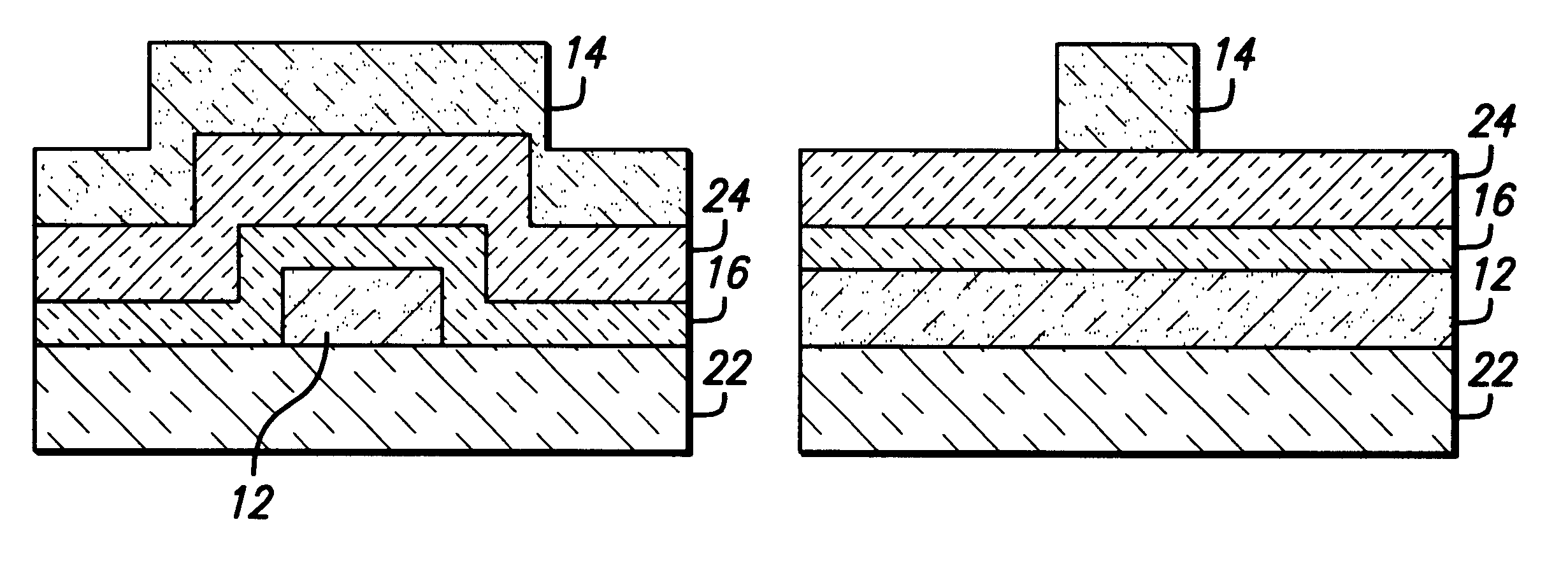
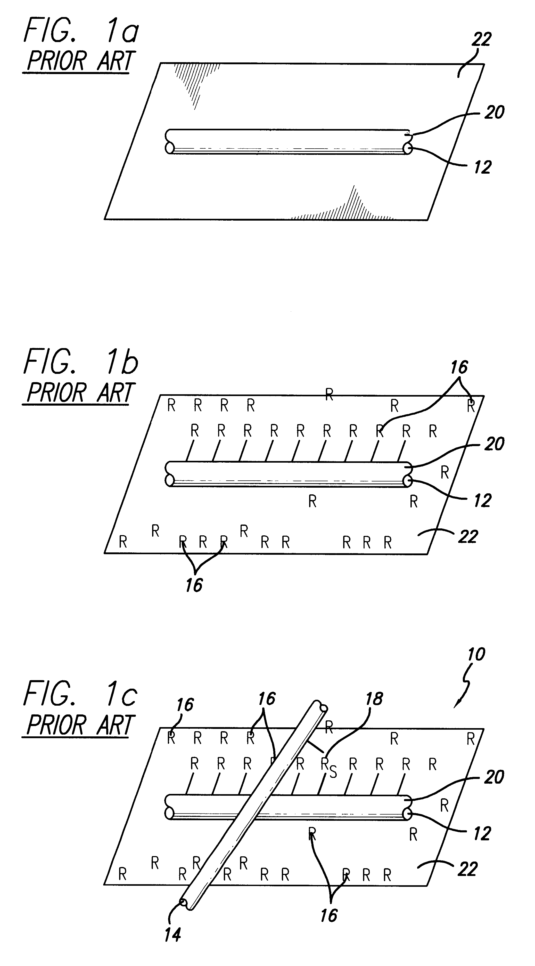
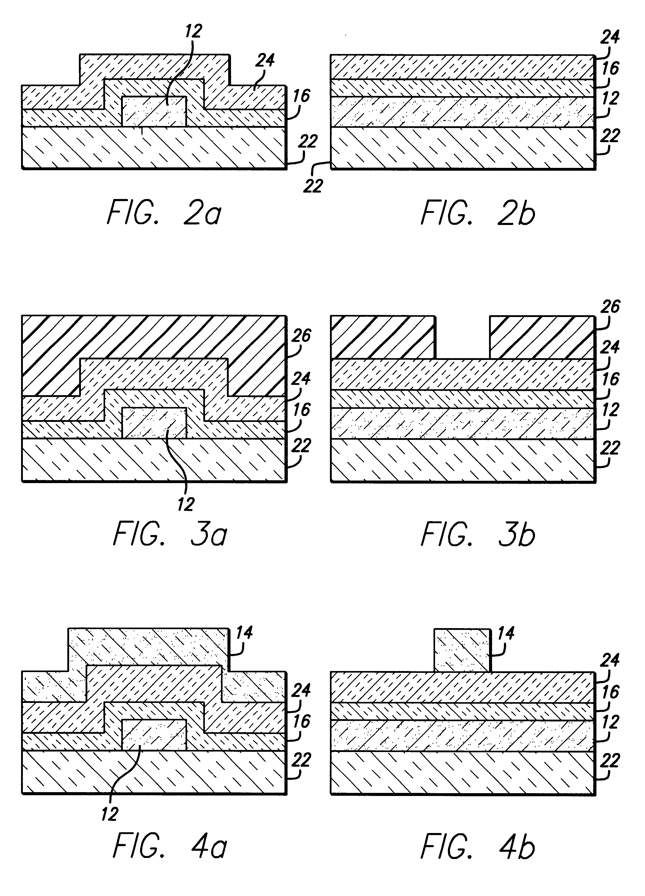
Embodiment Construction

Definitions

As used herein, the term "self-aligned" as applied to "junction" means that the junction that forms the switch and / or other electrical connection between two wires is created wherever two wires, either of which may be coated or functionalized, cross each other, because it is the act of crossing that creates the junction.

The term "self-assembled" as used herein refers to a system that naturally adopts some regular pattern because of the identity of the components of the system; the system achieves at least a local minimum in its energy by adopting this configuration.

The term "singly configurable" means that a switch can change its state only once via an irreversible process such as an oxidation or reduction reaction; such a switch can be the basis of a programmable read-only memory (PROM), for example.

The term "reconfigurable" means that a switch can change its state multiple times via a reversible process such as an oxidation or reduction; in other words, the switch can b...


PUM


Abstract

A method of fabricating a molecular electronic device or crossbar memory device is provided. The device comprises at least one pair of crossed wires and a molecular switch film therebetween. The method comprises: (a) forming at least one bottom electrode on a substrate by first forming a first layer on the substrate and patterning the first layer to form the bottom electrode by an imprinting technique; (b) forming the molecular switch film on top of the bottom electrode; (c) optionally forming a protective layer on top of the molecular switch film to avoid damage thereto during further processing; (d) coating a polymer layer on top of the protective layer and patterned the polymer layer by the imprinting method to form openings that expose portions of the protective layer; and (e) forming at least one top electrode on the protective layer through the openings in the polymer layer by first forming a second layer on the polymer layer and patterning the second layer. The imprinting method can be used to fabricate nanoscale patterns over a large area at high speeds acceptable in industrial standards. Consequently, it can be used to fabricate nanoscale molecular devices, e.g., crossbar memory circuits.

Description

The present application is generally directed to nanoscale computing and memory circuits, and, more particularly, to the formation of wires for device applications, specifically, use of imprinting to form electrodes, devices, and circuits. By "nanoscale" is meant that either the vertical dimension or the electrical pathway between electrodes is measured in nanometers.With the constantly decreasing feature sizes of integrated-circuit devices, well-behaved devices are becoming increasingly difficult to design. The fabrication is also becoming increasingly difficult and expensive. In addition, the number of electrons either accessed or utilized within a device is decreasing, with increasing statistical fluctuations in the electrical properties. In the limit, device operation depends on a single electron, and traditional device concepts must change.Molecular electronics has the potential to augment or even replace conventional devices with electronic elements, can be altered by external...

Claims


Application Information

Patent Timeline
Patent Type & Authority Patents(United States)
IPC IPC(8): H01L27/00B82B3/00H01L27/10H01L29/06H01L51/05
CPCB82Y10/00H01L27/285Y10S977/887H10K19/202
Inventor CHEN, YONG
Owner HEWLETT PACKARD DEV CO LP
Why Eureka
Try Eureka