AC plasma display panel

Inactive Publication Date: 2002-11-12
PANASONIC CORP
View PDF18 Cites 76 Cited by
  • Summary
  • Abstract
  • Description
  • Claims
  • Application Information

AI Technical Summary

Problems solved by technology

In order to employ the AC color plasma display in a wide range of use such as in a television for home use in the prior art, a display driving performance may be, however, reduced even when an improved structure is employed for elevating an emission efficiency.
Accordingly, the write condition does not become uniform to make a flicker, or to generate write inferiority on the entire panel in an extreme case only to

Method used


Image

  • AC plasma display panel
  • AC plasma display panel
  • AC plasma display panel

Examples


embodiment 1

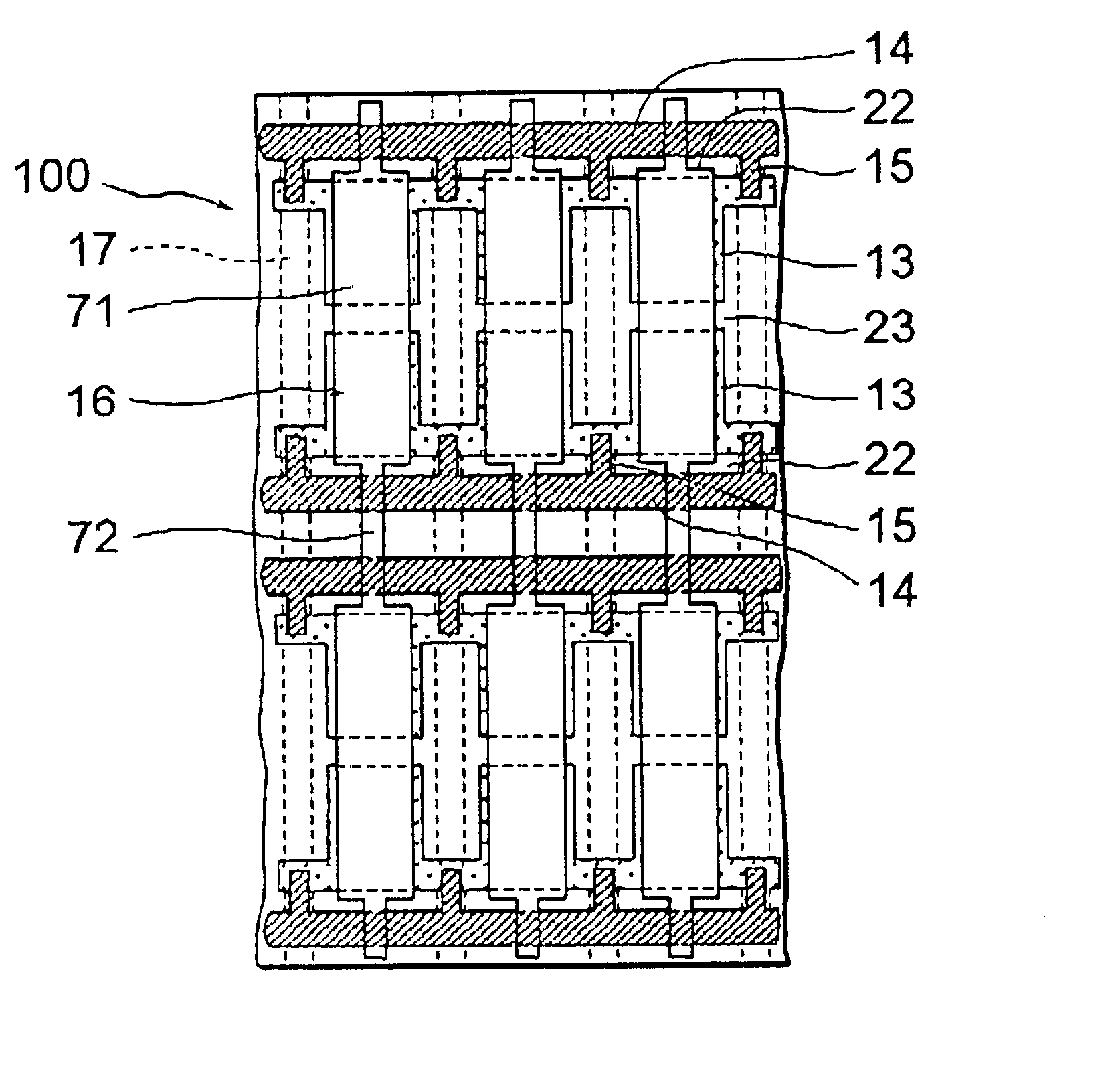
As shown in FIG. 5, an AC-PDP includes a pair of glass substrates 11 and 12, transparent electrodes 13, bus electrodes 14, coupling parts 15, data electrodes 16 and partition walls 17. The AC-PDP is fabricated as follows.

An ITO (indium-tin oxide) film is formed by sputtering on the glass substrate 11 functioning as a front surface substrate 110, and the transparent electrode 13 having comb-like projections as shown in FIG. 5 is formed by means of a photo-lithographic technique. The bus electrode 14 is formed to extend parallel to the transparent electrode 13 at the side of the transparent electrode 13 opposite to a surface discharging gap 23. A space 22 is formed between the transparent electrode 13 and the bus electrode 14. A plurality of the coupling parts 15 of the transparent electrode 13 projecting towards the bus electrode 14 are formed at a constant pitch on the transparent electrode 13, and the transparent electrode 13 and the bus electrode 14 are electrically connected to e...

embodiment 2

As shown in FIG. 7, the AC-PDP of Embodiment 2 has transparent electrodes 13A having an isolated structure. Embodiment 2 corresponds to a case where the coupling bar 62 exists only on one side of the discharge part 61. Although a dark defect may be generated when the electrode pattern has a defect, and shortcut or breakdown of the transparent electrode 13 cannot be electrically inspected because the projection 63 with the bus electrode 14 exists only on one side, an emission efficiency can be further improved because the coupling bar 62 exists only on one side. When an ability of manufacturing the transparent electrode pattern is high, the transparent electrode of FIG. 7 is effectively employed to elevate the emission efficiency.

Since the AC-PDP of Embodiment 2 is constituted as described above, the following effects can be obtained in addition to the effects of Embodiment 1.

Since the coupling bar 62 exists only on one side, the emission efficiency can be further improved.

When the a...

embodiment 3

In the AC-PDP of Embodiment 3 shown in FIG. 8, the coupling bar 62A and the projection 63 which act as the coupling part 15A are formed as a part of the pattern of the bus electrode 14A. In Embodiment 3, the bus electrode 14A may not extend to the coupling bar 62A, and it may include only the projection 63. The formation of the projection 63 and the coupling bar 62A as a part of the bus electrode 14A is useful when the transparent electrode 13 is a thin film which is liable to be breakdown due to a fine crack.


PUM


Abstract

Described herein is an AC plasma display panel in which a discharge part is separated from a bus electrode and a partition wall. In this AC plasma display panel, a high emission efficiency can be obtained. Also described is another AC plasma display panel in which a data electrode having a large width part around the surface discharging gap and a narrow width part. The data electrode may further include a medium width part. In this AC plasma display panel, since counter discharge always occurs near a discharge gap of a scanning electrode by employing the data electrode having a specified shape, a high resolution panel with full-color display can be realized.

Description

(a) Field of the InventionThe present invention relates to an AC plasma display panel (AC-PDP) for use in a flat panel television set and in a flat panel display unit, more in detail to the AC-PDP which realizes a high emission efficiency and improves display drive performance.(b) Description of the Related ArtA color plasma display excites a fluorescent substance to make an emission display by means of a ultraviolet ray generated by gas discharge, and an application of the display panel to a large-screen television set is expected. Various systems have been developed for the color PDPs among which a reflection-type AC coplanar switching plasma display panel (AC-IPS-PDP) is excellent in its brightness and ease of manufacture.FIGS. 1A to 1C show a typical reflection-type ACIPS-IPS-PDP. FIG.1A is an elevational view partially in section of a rear substrate, FIG. 1B is a side sectional view of a front substrate and FIG. 1C is a horizontal sectional view of the rear substrate.A front su...

Claims


Application Information

Patent Timeline
IPC IPC(8): H01J17/49
CPCH01J11/12H01J11/32H01J2211/245H01J2211/265H01J2211/323
Inventor NUNOMURA, KEIJI
Owner PANASONIC CORP
Why Eureka
Try Eureka