Vertical sub-micron CMOS transistors on (110), (111), (311), (511), and higher order surfaces of bulk, SOI and thin film structures and method of forming same

a technology of submicron cmos transistors and transistors, which is applied in the direction of transistors, electrical devices, semiconductor devices, etc., can solve the problems of difficult control of active and parasitic device threshold voltages

Inactive Publication Date: 2002-11-19
APTINA IMAGING CORP
View PDF10 Cites 263 Cited by
  • Summary
  • Abstract
  • Description
  • Claims
  • Application Information

AI Technical Summary

Problems solved by technology

The difference between high and low surface state densities was originally a particularly important consideration for NMOS technology in that a h

Method used


Image

  • Vertical sub-micron CMOS transistors on (110), (111), (311), (511), and higher order surfaces of bulk, SOI and thin film structures and method of forming same
  • Vertical sub-micron CMOS transistors on (110), (111), (311), (511), and higher order surfaces of bulk, SOI and thin film structures and method of forming same
  • Vertical sub-micron CMOS transistors on (110), (111), (311), (511), and higher order surfaces of bulk, SOI and thin film structures and method of forming same

Examples


Embodiment Construction

Illustrative embodiments and exemplary applications will now be described with reference to the accompanying drawings. The present invention describes the use of vertical device structures to achieve the advantages noted above as well as further advantages of the present invention.

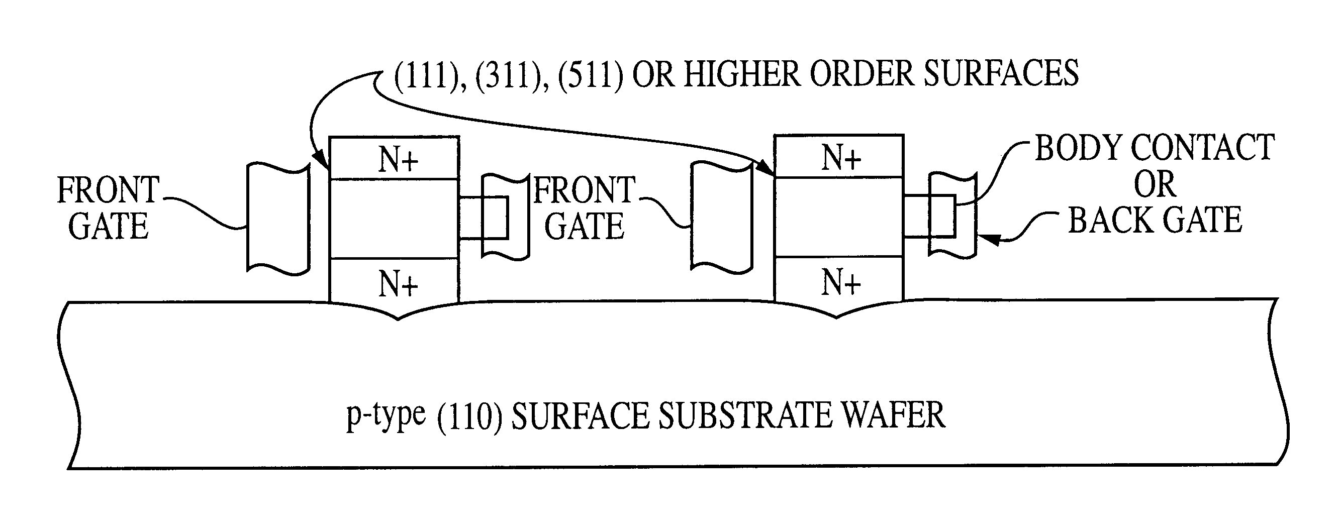
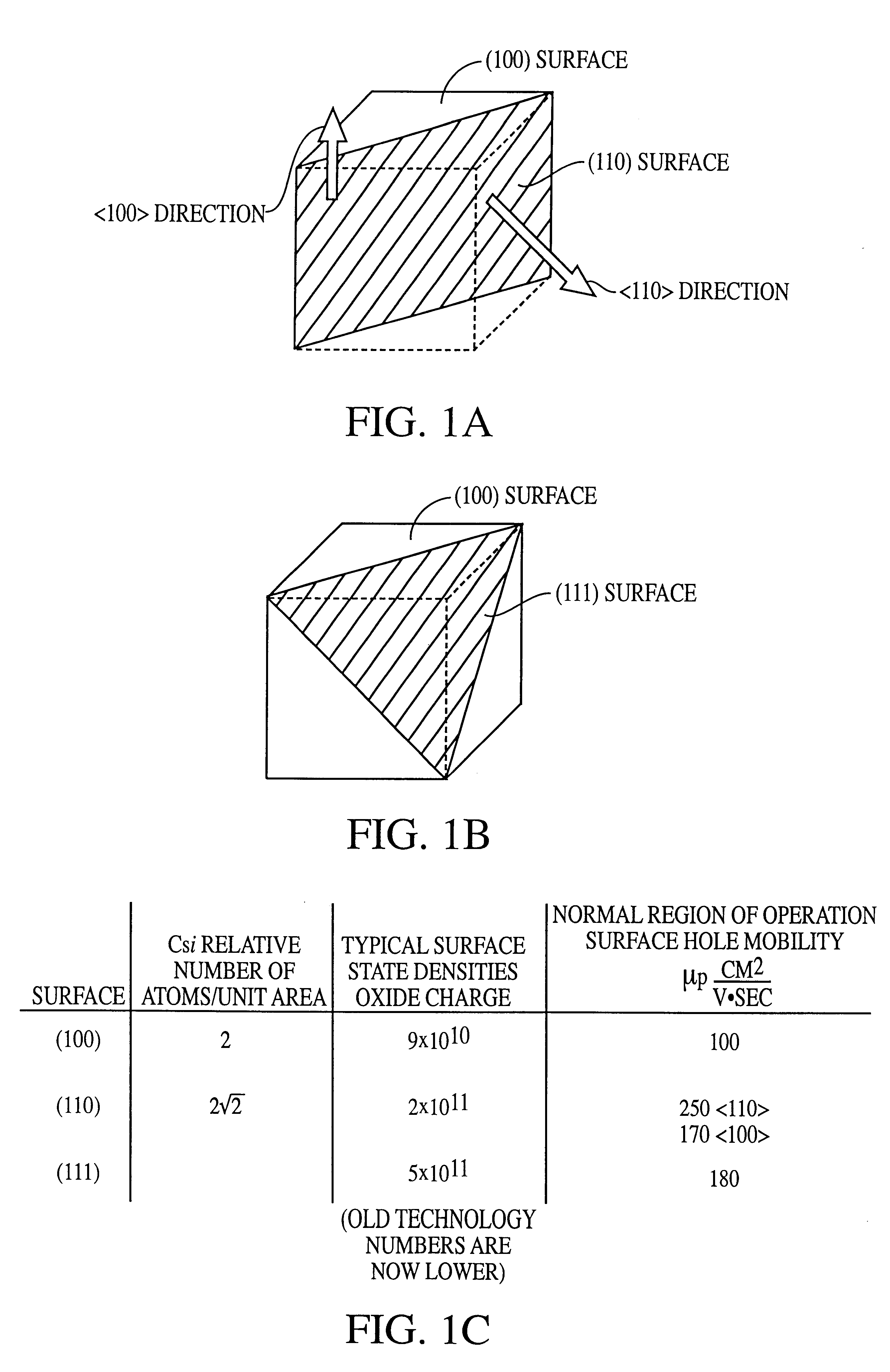
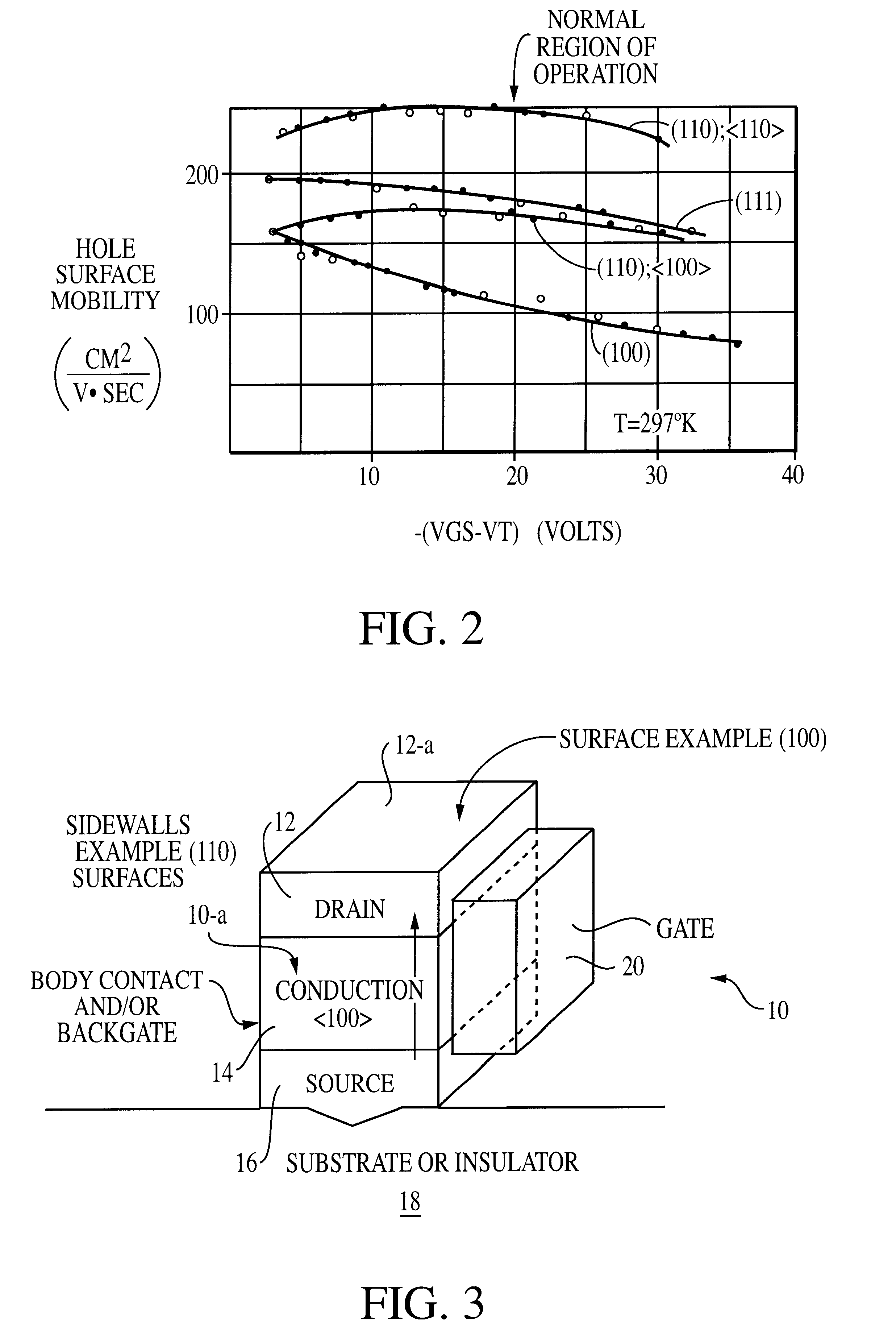
FIG. 3 illustrates an example of a vertical device 10, used in logic or memory applications. Vertical device 10 is formed on the sidewalls of intersecting trenches. As shown in FIG. 3, device 10 includes, from top to bottom, a drain 12, a conduction area 14, and a source 16, all of which are formed on a substrate or insulator 18. Gate 20 is formed on the side of the device 10. In the pictured example, the upper drain surface 12-a is formed on a (100) crystal orientation. As shown by the arrow, conduction occurs in the direction, from the source to the drain. The sidewalls 10-a of the device 10 are in this example formed on a (110) crystal orientation. Such devices as that pictured at 10 in FIG. 3 have the...


PUM


Abstract

A method for forming NMOS and PMOS transistors that includes cutting a substrate along a higher order orientation and fabricating deep sub-micron NMOS and PMOS transistors on the vertical surfaces thereof. The complementary NMOS and PMOS transistors form a CMOS transistor pair. The transistors are preferably used in structures such as memory circuits, e.g., DRAMs, which are, in turn, used in a processor-based system. Ideally, the deep sub-micron NMOS and PMOS transistors are operated in velocity saturation for optimal switching operation.

Description

1. Field of the InventionThe present invention relates to a method of improving hole mobility and thus velocity saturating vertical transistors by forming the vertical transistors on crystal surfaces of higher order. Also, the present invention deals with the method of forming the vertical transistors and their use in memory cells.2. Description of the Related ArtThe nearly universal standard silicon wafer crystal orientation for VLSI ("Very Large Scale Integration") is the (100) orientation. This orientation was chosen over the previously used (111) orientation due to its low surface state density on thermally oxidized surfaces, 9.times.10.sup.10 / cm.sup.2 versus 5.times.10.sup.11 / cm.sup.2 as shown in FIG. 1C. FIGS. 1A and 1B simply illustrate conventional crystal orientations.The difference between high and low surface state densities was originally a particularly important consideration for NMOS technology in that a high surface state density makes it difficult to control active...

Claims


Application Information

Patent Timeline
IPC IPC(8): H01L29/786H01L27/12H01L21/70H01L21/8238H01L29/02H01L29/66H01L29/04
CPCH01L21/823807H01L21/823885H01L27/1203H01L29/045H01L29/78639H01L29/78642H01L29/78648
Inventor FORBES, LEONARDNOBLE, WENDELL P.REINBERG, ALAN R.
Owner APTINA IMAGING CORP
Why Eureka
Try Eureka