Electronic assembly having a wetting layer on a thermally conductive heat spreader

a technology of thermally conductive heat spreader and wetting layer, which is applied in the direction of electrical apparatus, semiconductor devices, semiconductor/solid-state device details, etc., can solve the problem of low thermal conductivity

Inactive Publication Date: 2003-01-07
INTEL CORP
View PDF35 Cites 136 Cited by
  • Summary
  • Abstract
  • Description
  • Claims
  • Application Information

AI Technical Summary

Benefits of technology

Integrated circuits are manufactured on semiconductor wafers which are subsequently sawed or "diced" into individual dice. Such a die may have solder bump contacts on the integrated circuit. The solder bump contacts are located downward onto contact pads of a package substrate, and attached in a thermal reflow process. Electronic signals can be provided through the solder bump contacts to and from the integrated circuit. Operation of the integrated circuit causes heating thereof. Heat is conducted to an upper surface of the die, and has to be conducted or convected away to maintain the temperature of the integrated circuit below a predetermined level for purposes of maintaining functional integrity of the integrated circuit.

Problems solved by technology

Such a die may have solder bump contacts on the integrated circuit.
Operation of the integrated circuit causes heating thereof.
The thermally conductive grease transfers minimal stresses from the heat spreader to the die, but has a relatively low thermal conductivity and thus provides a substantial barrier for heat transferring from the die to a heat spreader.

Method used


Image

  • Electronic assembly having a wetting layer on a thermally conductive heat spreader
  • Electronic assembly having a wetting layer on a thermally conductive heat spreader
  • Electronic assembly having a wetting layer on a thermally conductive heat spreader

Examples


Embodiment Construction

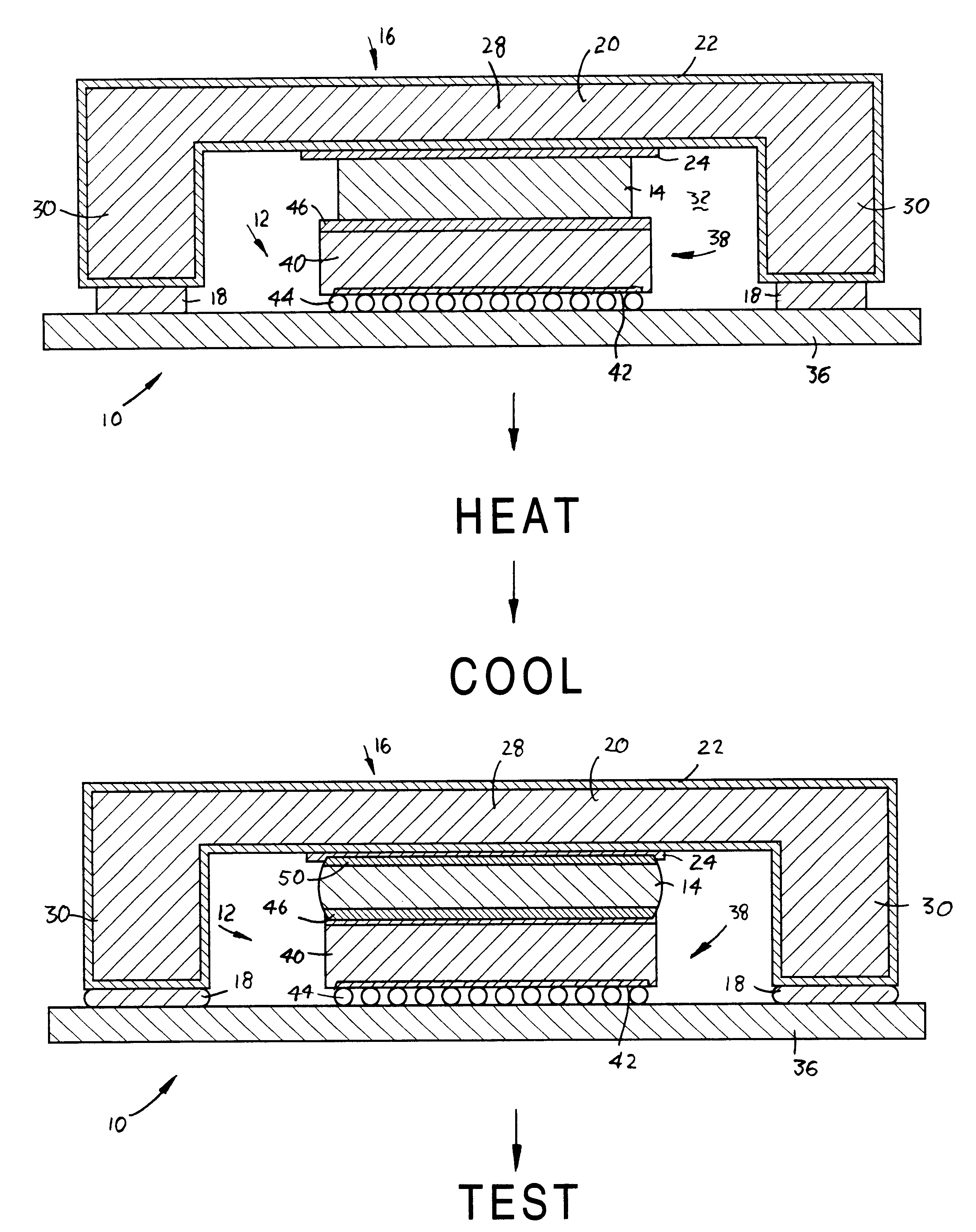
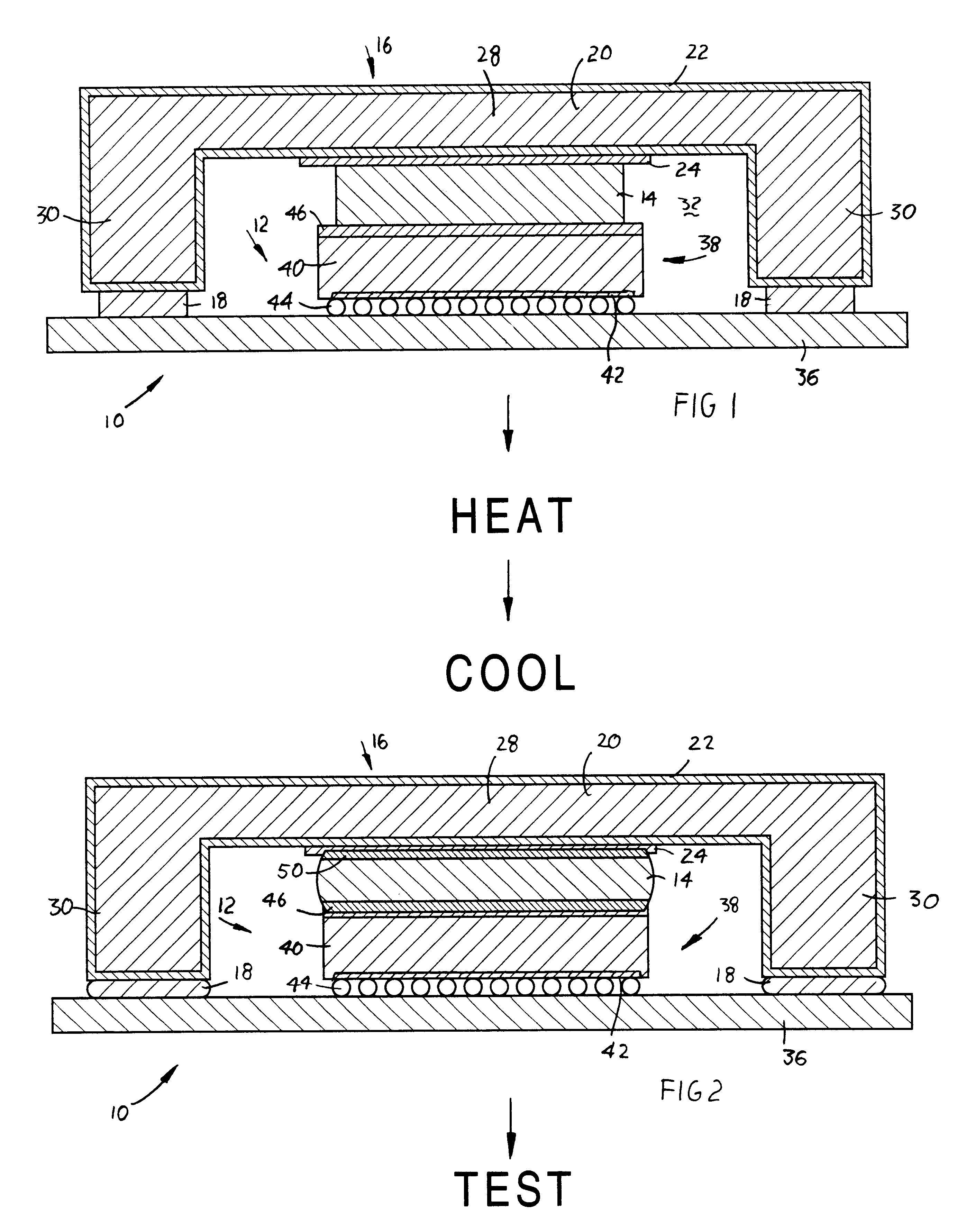
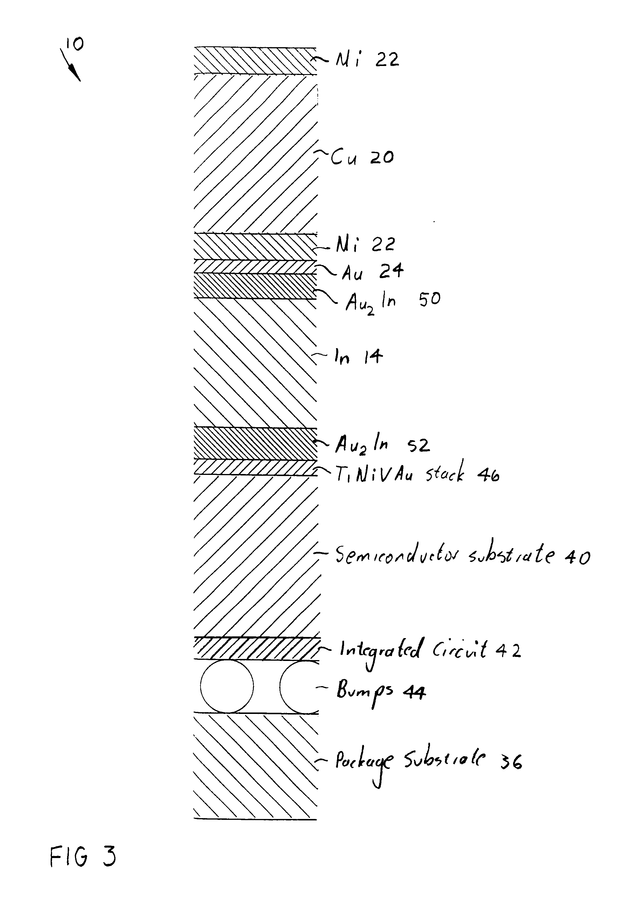
FIG. 1 of the accompanying drawings illustrates components of an electronic assembly 10, before being finally assembled, including a semiconductor package subassembly 12, a preform of pure indium 14, a heat spreader subassembly 16, and an adhesive 18.

The heat spreader subassembly 16 includes a primary heat spreading structure 20 of copper, a thin nickel layer 22 plated on the primary heat spreading structure 20, and a gold layer 24 plated on the nickel layer 22.

The primary heat spreading structure 20 includes a horizontal heat spreading plate 28, and sides 30 extending downward from edges of the heat spreading plate 28. There are four of the sides 30 which, together with the heat spreading plate 28, form an inverted cap with an internal cavity 32 which is open to the bottom. All surfaces of the primary heat spreading structure 20 are plated with the nickel layer 22. The nickel layer 22 is thus also plated on a lower surface of the heat spreading plate 28.

The gold layer 24 is selecti...


PUM

PropertyMeasurementUnit
thickaaaaaaaaaa
thickaaaaaaaaaa
thickaaaaaaaaaa

Abstract

An electronic assembly including a die, having an integrated circuit formed therein, a thermally conductive heat spreader, and indium located between the die and the heat spreader, is described. The heat spreader has a layer of nickel. A gold layer is formed on the nickel layer, and provides better wetting of indium than nickel. A better structural connection between the indium and the heat spreader is provided, especially during thermal cycling.

Description

BACKGROUND OF THE INVENTION1). Field of the InventionThis invention relates to an electronic assembly of the kind having a semiconductor die which is thermally coupled through an interface material to a thermally conductive heat spreader.2). Discussion of Related ArtIntegrated circuits are manufactured on semiconductor wafers which are subsequently sawed or "diced" into individual dice. Such a die may have solder bump contacts on the integrated circuit. The solder bump contacts are located downward onto contact pads of a package substrate, and attached in a thermal reflow process. Electronic signals can be provided through the solder bump contacts to and from the integrated circuit. Operation of the integrated circuit causes heating thereof. Heat is conducted to an upper surface of the die, and has to be conducted or convected away to maintain the temperature of the integrated circuit below a predetermined level for purposes of maintaining functional integrity of the integrated circ...

Claims


Application Information

Patent Timeline
Patent Type & Authority Patents(United States)
IPC IPC(8): H01L23/34H01L23/373
CPCH01L23/3736H01L23/433H01L24/31H01L23/3735H01L23/10H01L2224/0401H01L2224/04026H01L2224/16227H01L2224/73253H01L2924/01013H01L2924/01029H01L2924/01033H01L2924/01046H01L2924/01047H01L2924/01049H01L2924/0105H01L2924/01074H01L2924/01078H01L2924/01079H01L2924/01327H01L2924/12044H01L2924/14H01L2924/16152H01L2924/01006H01L2924/01023H01L2924/0132H01L2224/16225H01L2924/01028H01L2924/3512H01L2924/00
Inventor DEPPISCH, CARL L.HOULE, SABINA J.FITZGERALD, THOMAS J.DAYTON, KRISTOPHER E.HUA, FAY
Owner INTEL CORP
Why Eureka
Try Eureka