RF power divider/combiner circuit

a power divider and combinator technology, applied in the field of rf communication, can solve problems such as increased vswr and insertion loss, increased insertion loss, and difficulty in solving problems

Inactive Publication Date: 2003-02-11
SIGNAL TECH CORP
View PDF4 Cites 55 Cited by
  • Summary
  • Abstract
  • Description
  • Claims
  • Application Information

AI Technical Summary

Benefits of technology

Still another object of this invention is to provide an RF power divider / combiner that exhibits low insertion losses for a wide range of operating power.
In accordance with one aspect of this invention, a power combiner circuit for RF signals includes a multi-path network for conveying RF signals from a plurality of RF sources to a common node. A switched RF impedance transformer between the common node and an RF load switches between first and second transformation functions depending upon the number of sources that are active simultaneously thereby to minimize any impedance mismatch between the common node and the RF load.

Problems solved by technology

With parallel, identical, lower powered amplifiers, however, the problem becomes more difficult because the output impedance of the collective amplifiers will be Z.sub.0 / N where Z.sub.0 is the characteristic impedance of one amplifier and N is the number of amplifiers operating in parallel.
If the impedance is not well matched, VSWR and insertion losses increase.
Insertion losses when only one amplifier is operating can become 75% of the input.
With these losses it can be seen, particularly if equal amplitudes and phases are not maintained, that significant heat will be generated.
In systems using resistors, this heat can lead to circuit failure.
Therefore it appears that in this system a wide range of mismatches can still occur.
While this system appears to optimize for a particular configuration in anticipation of a failure of one path, it does not appear readily adapted for providing for optimal impedance if more than one channel becomes inactive.
Examination of each of the foregoing patents and other prior art that is representative of prior art indicates that each of the approaches is overly complex.
As a result problems of heating and insertion losses and impedance mismatches continue to exist.

Method used


Image

  • RF power divider/combiner circuit
  • RF power divider/combiner circuit
  • RF power divider/combiner circuit

Examples


Embodiment Construction

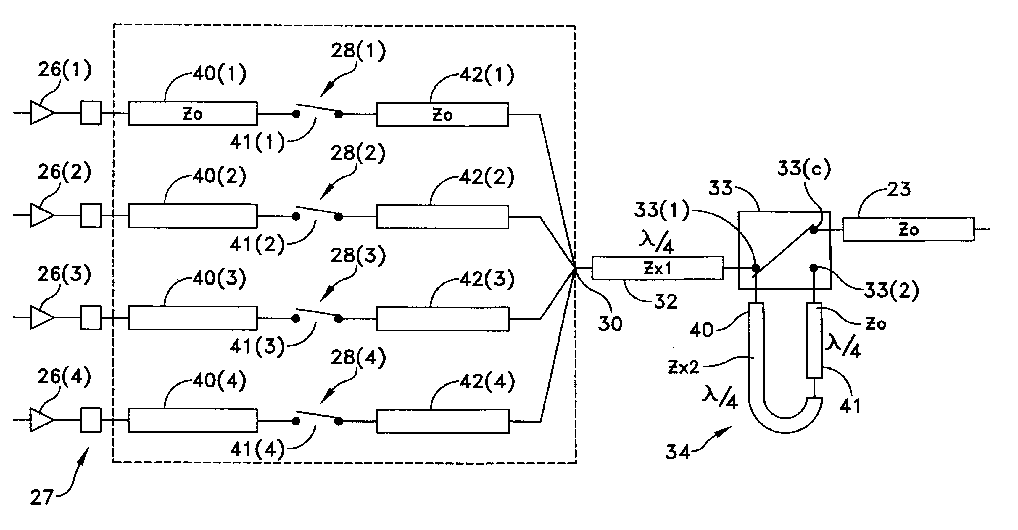
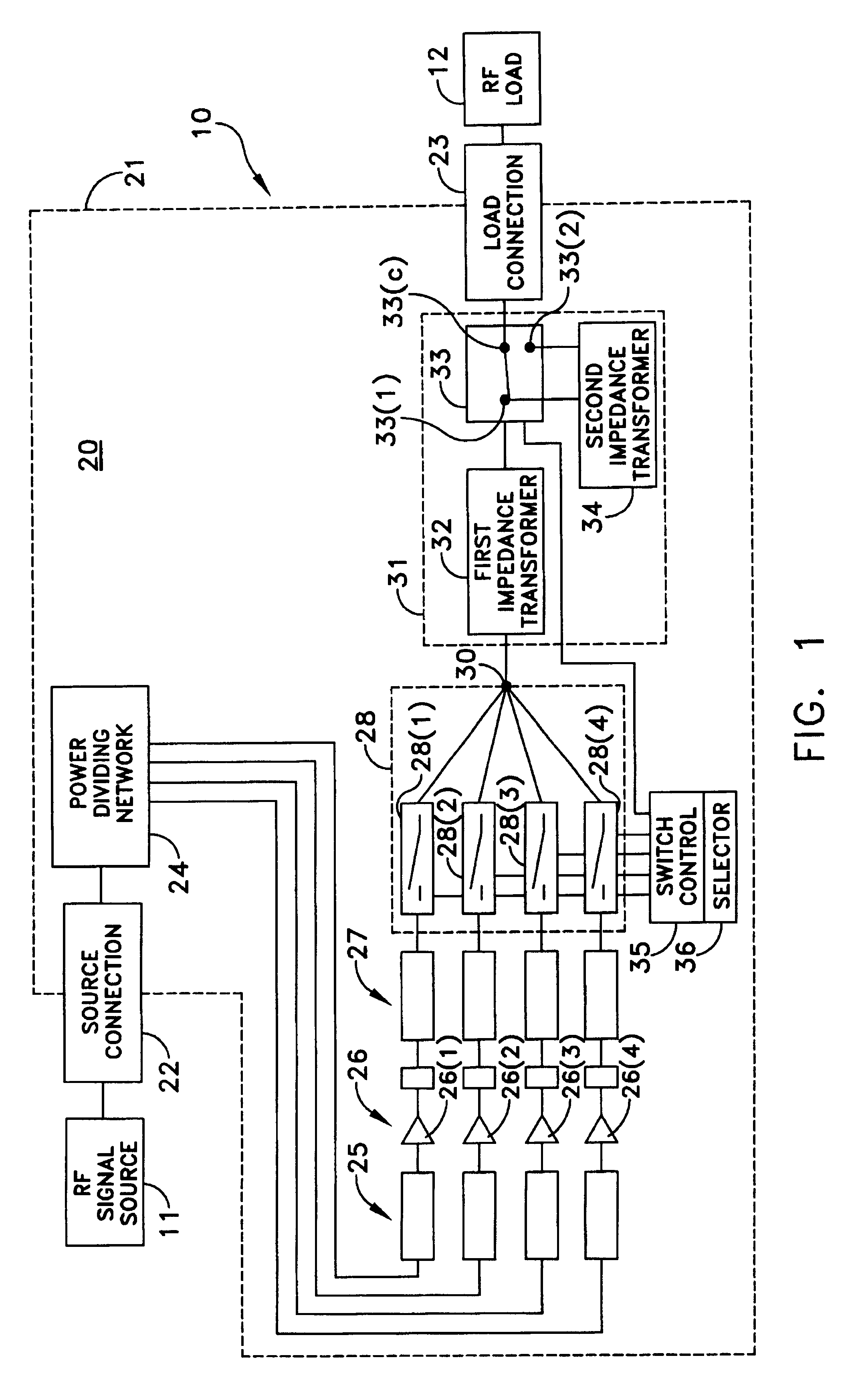
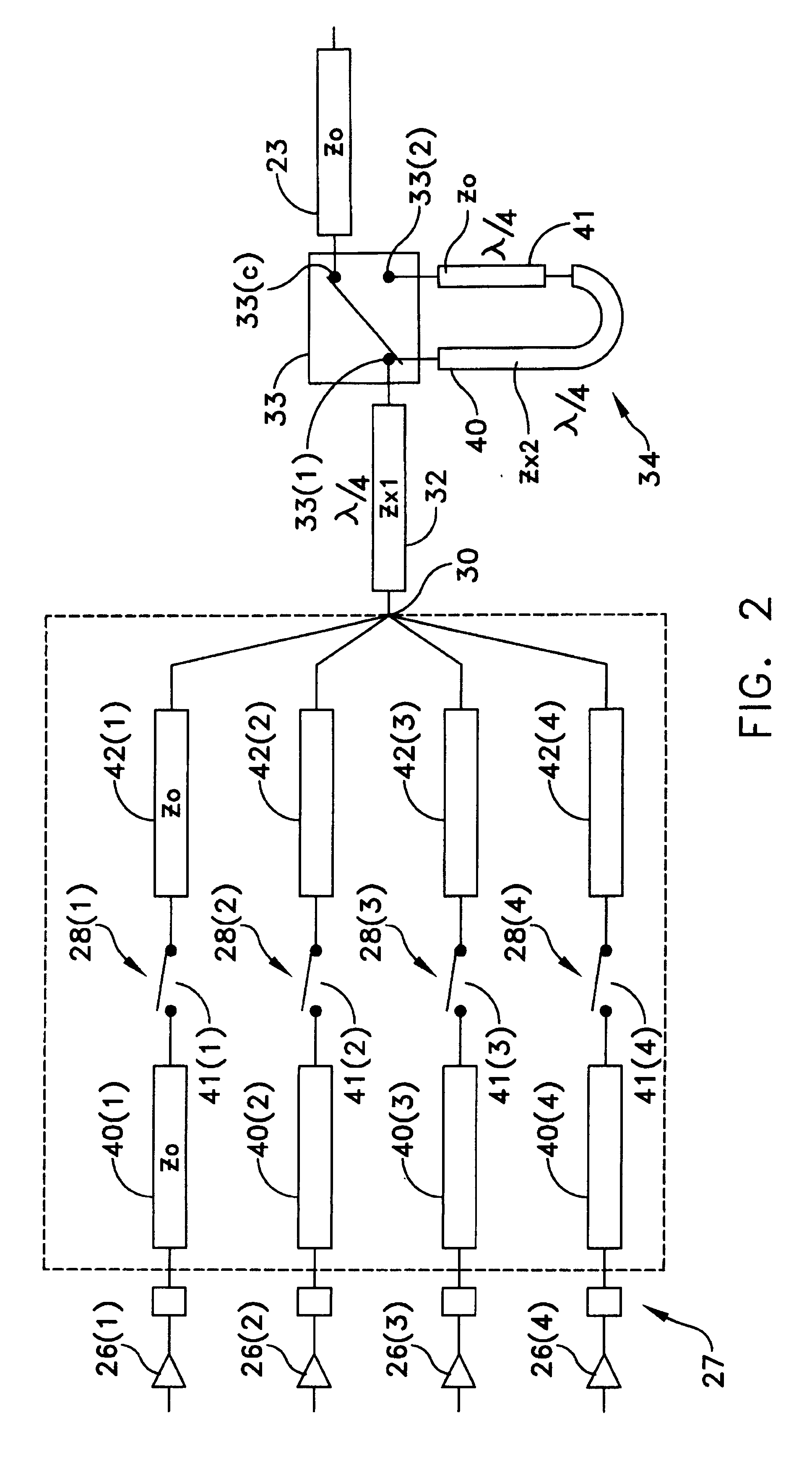
FIG. 1 depicts an RF system 10 that includes an RF signal source 11 and an RF load 12. A power divider / combiner circuit 20 includes a grounded chassis 21, a source connection 22 for receiving signals from the RF signal source and a load connection 23 for providing signals to the RF load 12. The source and load connections 22 and 23 typically will be constituted by coax feed-through couplings for receiving a connector on a transmission line from the RF signal source 11 or from the RF load 12. However, the source and load connections 22 and 23 could be any variety of connection.

A power dividing network can take any of several conventional forms that will divide the signal appearing at the source connection 22 into equi-phase, equi-amplitude signals. For an N-way power combiner circuit the division is into N paths. N=4 is a typical value and is used in the following discussion. Specifically, FIG. 1 depicts four such paths to a series of amplifier input connections 25. These amplifier i...


PUM


Abstract

A power combiner circuit for RF signals includes a multi-path network for conveying a plurality of RF signals over a selected path or paths, to a common node. A switched RF impedance transformer connects between the common node and an RF load. The switched RF transformer switches between first and second transformation functions depending upon the number of network paths that are selected.

Description

1. Field of the InventionThis invention generally relates to RF communications and more specifically to an N-way divider / combiner that facilitates the control of a transmitted RF signal.2. Description of Related ArtWireless RF applications, particularly in the 800 to 1000 MHz range, have become wide spread in recent years. These are frequencies of choice for wireless telephones and similar devices. Particular effort has been directed to the development of the high-power RF transmitting facilities for such applications including wireless telephone repeaters.Many of these applications include multiple amplifiers to provide an appropriate RF output power. For example, a 600 watt transmitting facility may include four 150 watt transmitters operating in parallel, rather than a single 600 watt transmitter. Using lower powered amplifiers provides reliability through redundancy and, in many cases reduced costs as the cost of several lower powered RF amplifiers may be less than a single high...

Claims


Application Information

Patent Timeline
Patent Type & Authority Patents(United States)
IPC IPC(8): H01P5/12H01P5/04
CPCH01P5/12H01P5/04H01P5/16
Inventor CASALE, THOMAS J.ARLIN, STEVEN
Owner SIGNAL TECH CORP
Why Eureka
Try Eureka