Etch stop barrier for stencil mask fabrication
- Summary
- Abstract
- Description
- Claims
- Application Information
AI Technical Summary
Benefits of technology
Problems solved by technology
Method used
Image

Examples
Embodiment Construction
)
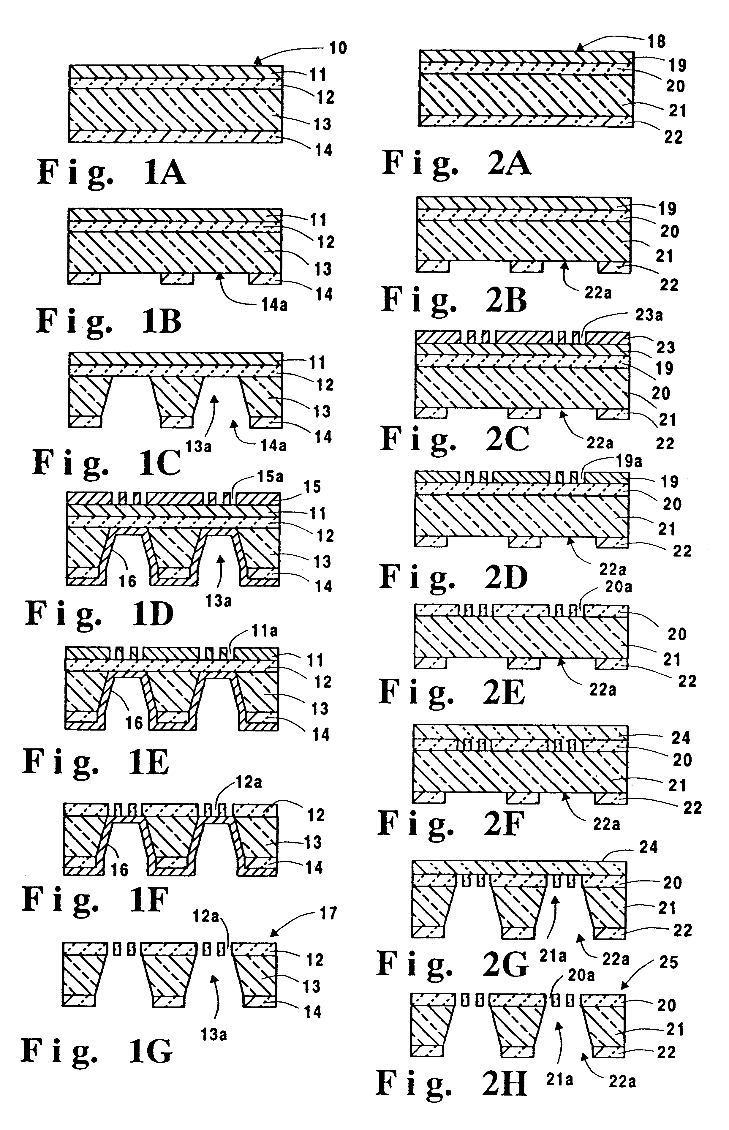
In describing the preferred embodiment of the present invention, reference will be made herein to FIGS. 1A-2H of the drawings in which like numerals refer to like features of the invention. Features of the invention are not necessarily shown to scale in the drawings.
Referring first to FIGS. 1A-1G a method of the invention for making a stencil mask is shown.
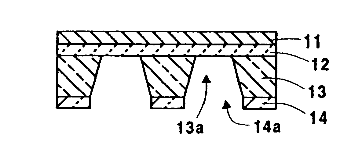
In FIG. 1A a substrate for making a mask is shown in composite as numeral 10. The mask substrate comprises, in sequential layers from the bottom layer to the top layer, a backside hardmask layer 14, a silicon substrate layer 13, a stencil pattern forming layer 12 and a top frontside hard mask layer 11. The backside hardmask layer 14 is typically silicon nitride, silicon carbide or boron-doped silicon. Silicon nitride and silicon carbide are typically formed on the substrate 13 by chemical vapor eposition (CVD) and boron doped silicon by diffusion. The backside hardmask layer 4 is generally about 0.2 to 5 .mu.m thick. The substrat...
PUM
 Abstract
Description
Claims
Application Information
 - R&D Engineer
- R&D Manager
- IP Professional
- Industry Leading Data Capabilities
- Powerful AI technology
- Patent DNA Extraction
Browse by: Latest US Patents, China's latest patents, Technical Efficacy Thesaurus, Application Domain, Technology Topic.
© 2024 PatSnap. All rights reserved.Legal|Privacy policy|Modern Slavery Act Transparency Statement|Sitemap