Array substrate for a liquid crystal display device and method for fabricating the same

a liquid crystal display and array substrate technology, applied in the direction of measurement devices, instruments, electrical testing, etc., can solve the problems of electrical defects, such as open- and short-circuit electrical defects, and assembly of dot defects and line defects,

Inactive Publication Date: 2003-06-10
LG DISPLAY CO LTD
View PDF6 Cites 161 Cited by
  • Summary
  • Abstract
  • Description
  • Claims
  • Application Information

AI Technical Summary

Problems solved by technology

However, mating small-sized array substrates together requires a relatively complex mating process. FIG. 3B is a plan view illustrating a conventional large LCD device 61.
During the fabrication of that large LCD device 61, electrical defects, such as open- and short-circuits, can occur during assembly.
Typical defects include dot defects and line defects.
For example, a dot defect is when a particular TFT does not operate when electrical signals are applied via the drive circuitry.
An example of a line defect is when all of the TFTs connected to a gate line (or to a data line) do not operate due to a shorted or open gate line (or data line).
However, with large-sized LCD devices, the economic loss that results from a defect can be much larger, at least partially because the manufacturing costs of large-sized LCD devices are so much higher.
Furthermore, the larger areas involved and the more difficult fabrication process cause large-sized LCD devices to generally have low manufacturing yields.

Method used


Image

  • Array substrate for a liquid crystal display device and method for fabricating the same
  • Array substrate for a liquid crystal display device and method for fabricating the same
  • Array substrate for a liquid crystal display device and method for fabricating the same

Examples


Embodiment Construction

Reference will now be made in detail to illustrated embodiments of the present invention, examples of which are shown in the accompanying drawings.

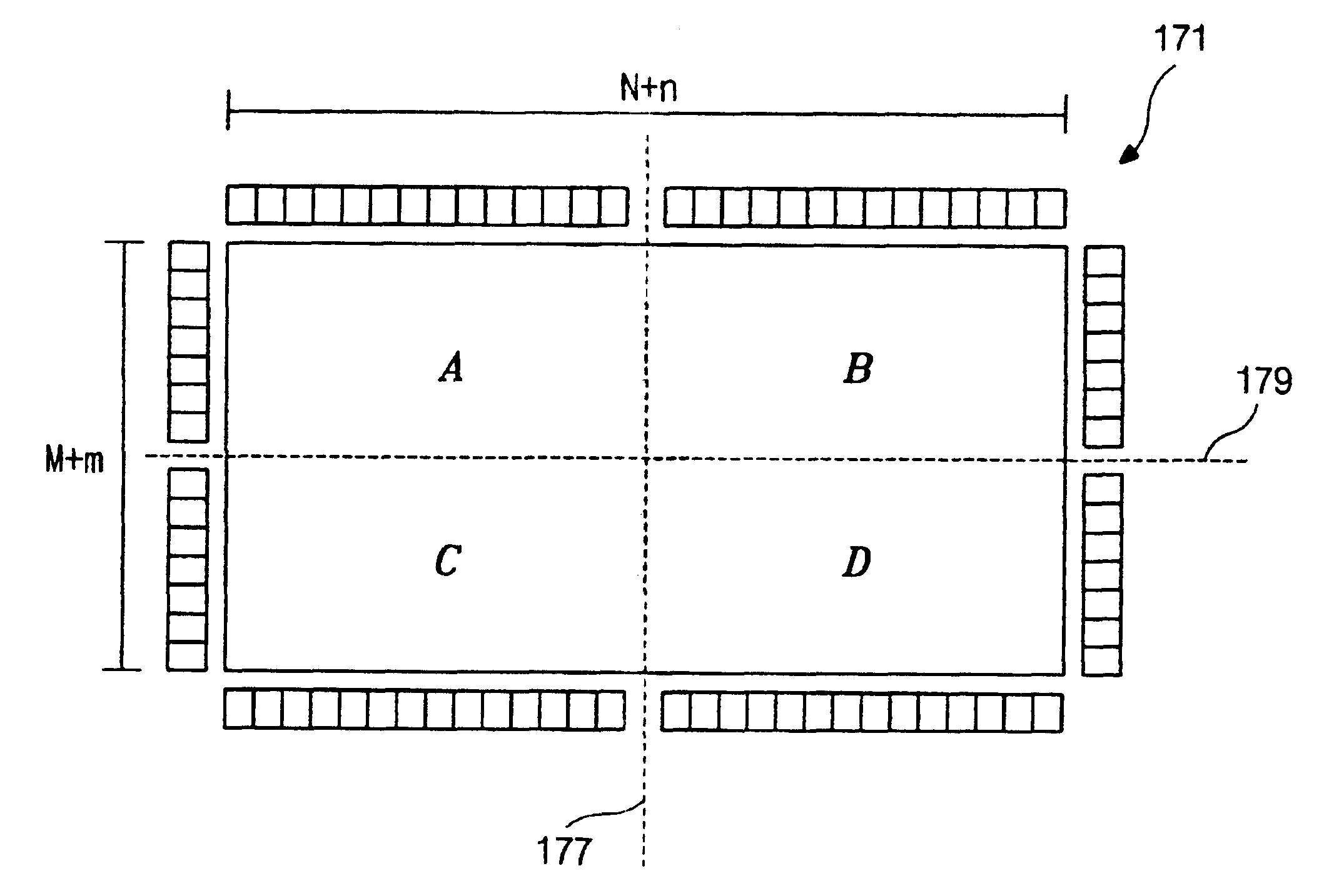
FIG. 4 is a plan view of an array substrate for a large-sized LCD device according to an embodiment of the present invention. Although the array substrate of FIG. 4 may look similar to the array substrate of FIG. 3B, those array substrates have different numbers of pixels. The array substrate of FIG. 4 includes (M+m).times.(N+n) pixels that are fabricated to form an M.times.N display. This is contrary to the conventional method of forming an array substrate for an M.times.N LCD device in which only M.times.N pixels are fabricated. Namely, redundant pixels are added. Moreover, if the redundant pixels are not required, they are disabled such that they do not impact the LCD device. Beneficially, to provide sufficient redundant pixels, m and n are greater than 10. To avoid wasting space, the number of the redundant pixels are beneficially les...


PUM

PropertyMeasurementUnit
electrical defectaaaaaaaaaa
sizeaaaaaaaaaa
electricalaaaaaaaaaa

Abstract

A method of fabricating LCD devices from large array substrates having redundant pixels. Large array substrates without defects can be used to fabricate large LCD device and the redundant pixels can be disabled. Large array substrates with defects can be cut into smaller array substrates and then used to form small LCD devices. The pixels around the cutting lines of the large array substrate are redundant and can be covered or disabled.

Description

This application claims the benefit of Korean Patent Application No. 2000-1339, filed on Jan. 12, 2000, under 35 U.S.C. .sctn.119, the entirety of which is hereby incorporated by reference.1. Field of the InventionThe present invention relates to a liquid crystal display (LCD) device. More particularly, it relates to an array substrate for use in a liquid crystal display device and a method of manufacturing the same.2. Description of Related ArtA liquid crystal display (LCD) device includes a display and a pad. The pad applies electrical signals to the display, and thus includes drive circuitry. The display produces an image. The display itself includes upper and lower substrates, and an interposed liquid crystal layer.FIG. 1 is a schematic perspective view illustrating a typical liquid crystal display (LCD) device 10. The LCD device 10 includes an upper substrate 11 and a lower substrate 17, which are opposed to and spaced apart from each other. A liquid crystal layer 19 is interpo...

Claims


Application Information

Patent Timeline
Patent Type & Authority Patents(United States)
IPC IPC(8): G02F1/1333G02F1/13G02F1/1362G02F1/1343G02F1/133
CPCG02F1/1309G02F1/133351G02F2201/123G02F1/136259G02F1/134336G02F1/133
Inventor KIM, SOO-MAHN
Owner LG DISPLAY CO LTD
Why Eureka
Try Eureka