Flat-type display

a display and type technology, applied in the field of flat-type display, can solve the problems of high technical difficulty in carrying out the above-mentioned particle control

Inactive Publication Date: 2003-06-17
SONY CORP
View PDF8 Cites 55 Cited by
  • Summary
  • Abstract
  • Description
  • Claims
  • Application Information

AI Technical Summary

Benefits of technology

It is therefore an object of the present invention to provide a flat-type display that permits reliable inhibition of discharges between the first panel and the second panel, so that display images on a screen are free from degradation.
In the flat-type display according to the first aspect of the present invention, the electron-emitting-portion cutoff circuit is provided between the electron-emitting portion and the electron-emitting-portion driving circuit for preventing a discharge between the electron-emitting portion and the electron irradiation surface. Even if a discharge takes place, therefore, the electron-emitting-portion cutoff circuit readily cuts off the electric connection between the electron-emitting portion and the electron-emitting-portion driving circuit. In the flat-type display according to the second aspect of the present invention, the anode-electrode cutoff circuit is provided between the anode electrode and the anode-electrode driving circuit for preventing a discharge between the electron-emitting portion and the electron irradiation surface. Even if a discharge takes place, therefore, the anode-electrode cutoff circuit readily cuts off the electric connection between the anode electrode and the anode-electrode driving circuit. In the flat-type display according to the third aspect of the present invention, the shield-member cutoff circuit is provided between the shield member and the shield-member voltage-applying means for preventing a discharge between the shield member and the electron irradiation surface. Even if a discharge takes place, therefore, the shield-member cutoff circuit readily cuts off the electric connection between the shield member and the shield-member voltage-applying means, so that no detrimental effect is caused on the shield-member voltage-applying means and further that no detrimental effect is caused on the electron-emitting portion and the electron-emitting-portion driving circuit.

Problems solved by technology

It involves high technical difficulties to carry out the above particle control in the process for producing the first panel or a display having the first panel.

Method used


Image

  • Flat-type display
  • Flat-type display
  • Flat-type display

Examples


example 1

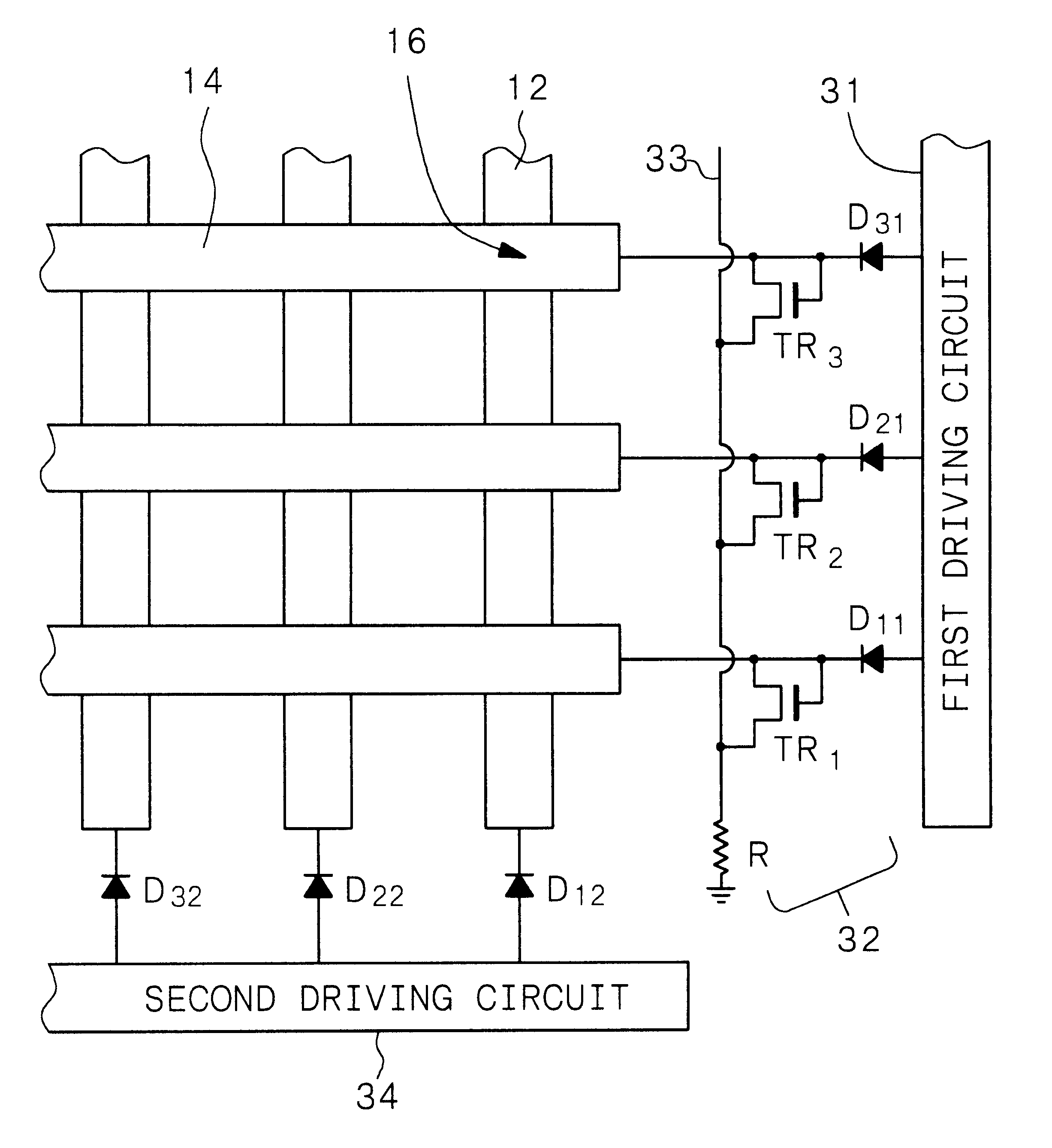
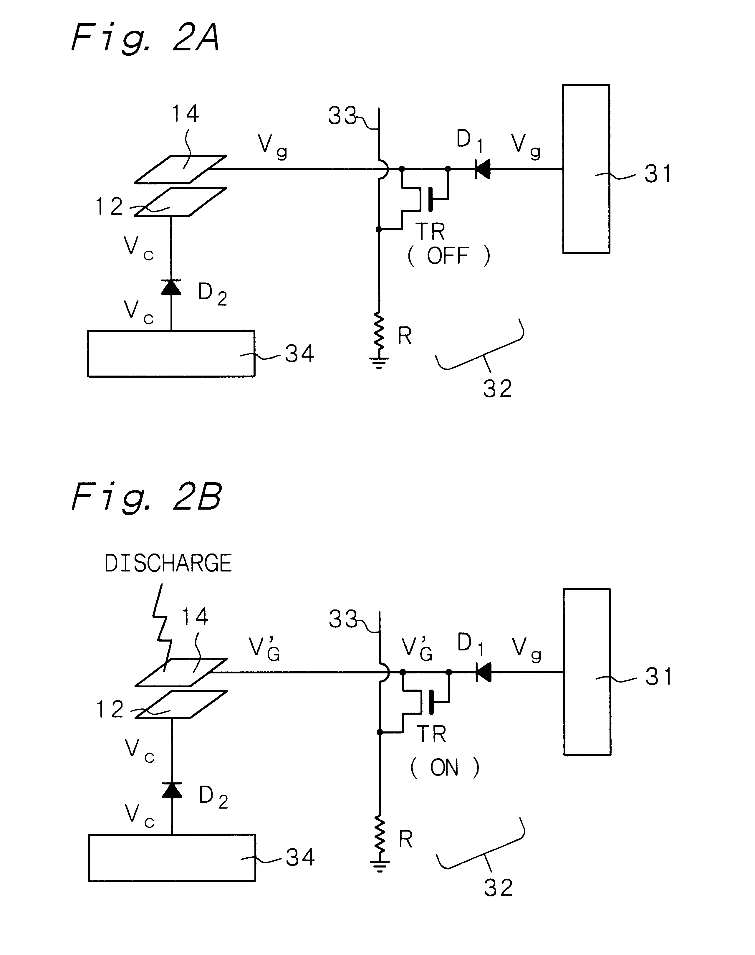
Example 1 is concerned with the flat-type display (more specifically, a cold cathode field emission display) according to the first aspect of the present invention, and further with the flat-type display according to the first constitution. FIG. 1 shows a conceptual drawing of the flat-type display of Example 1, and FIG. 3 shows a schematic partial end view thereof. The flat-type display comprises a first panel (cathode panel) 10 having electron-emitting portions 16, a second panel (anode panel) 20 having an electron irradiation surface, and electron-emitting-portion driving circuits 31 and 34 for driving the electron-emitting portions 16, and the flat-type display is provided with an electron-emitting-portion cutoff circuit between the electron-emitting portions 16 and the electron-emitting-portion driving circuit for preventing a discharge between the electron-emitting portions 16 and the electron irradiation surface. More specifically, the flat-type display of Example 1 has a str...

example 2

Example 2 is concerned with the flat-type display according to the first aspect of the present invention and further with the flat-type display according to the second constitution. FIG. 6 shows a conceptual drawing of the flat-type display of Example 2, and FIG. 8 shows a schematic partial end view thereof. The flat-type display comprises a stripe-shaped gate electrode 14 and a stripe-shaped cathode electrode 12 extending in a direction different from the extending direction of the stripe-shaped gate electrode 14, and the electron-emitting portion 16 is positioned in an overlap region where the projection image of the stripe-shaped gate electrode 14 and the projection image of the stripe-shaped cathode electrode 12 overlap. An electron-emitting-portion driving circuit comprises a first driving circuit 31 connected to the gate electrodes 14 and a second driving circuit 34 connected to the cathode electrodes 12. And, the second driving circuit 34 is connected to the cathode electrode...

example 3

Example 3 is concerned with the flat-type display according to the first aspect of the present invention and further with the flat-type display according to the third constitution. FIG. 9 shows a conceptual drawing of the flat-type display of Example 3, and FIG. 11 shows a schematic partial end view thereof. The flat-type display of Example 3 comprises a stripe-shaped gate electrode 14 and a stripe-shaped cathode electrode 12 extending in a direction different from the extending direction of the stripe-shaped gate electrode 14, and the electron-emitting portion 16 is positioned in an overlap region where the projection image of the stripe-shaped gate electrode 14 and the projection image of the stripe-shaped cathode electrode 12 overlap. An electron-emitting-portion driving circuit comprises a first driving circuit (gate-electrode driving circuit) 31 connected to the gate electrodes 14 and a second driving circuit (cathode-electrode driving circuit) 34 connected to the cathode elect...


PUM


Abstract

A flat-type display comprising a first panel having electron-emitting portions; a second panel having an electron irradiation surface; and an electron-emitting-portion driving circuit for driving the electron-emitting portions, wherein an electron-emitting-portion cutoff circuit is provided between the electron-emitting portions and the electron-emitting-portion driving circuit for preventing a discharge between the electron-emitting portions and the electron irradiation surface.

Description

BACKGROUND OF THE INVENTION AND RELATED ART STATEMENTThe present invention relates to a flat-type display such as a cold cathode field emission display.As an image display device that can be substituted for a currently mainstream cathode ray tube (CRT), flat-screen (flat-panel) displays are studied in various ways. Such flat-panel displays include a liquid crystal display (LCD), an electroluminescence display (ELD) and a plasma display (PDP). There has been also proposed a cold cathode field emission display capable of emitting electrons into a vacuum from a solid without relying on thermal excitation, a so-called a field emission display (FED), and it attracts attention from the viewpoint of the brightness of a display screen and low power consumption.FIG. 82 shows a typical constitution of the cold cathode field emission display (to be sometimes abbreviated as "display" hereinafter), and FIG. 83 shows a schematic exploded view of some portions of a first panel 10 and a second pane...

Claims


Application Information

Patent Timeline
Patent Type & Authority Patents(United States)
IPC IPC(8): G09G3/22H01J29/00H01J29/96H01J31/12H01J1/304G09G3/20H01J1/30
CPCG09G3/22H01J31/127H01J29/96H01J1/30
Inventor KONISHI, MORIKAZUIIDA, KOICHI
Owner SONY CORP
Why Eureka
Try Eureka