Apparatus for biasing ultra-low voltage logic circuits

a logic circuit and ultra-low voltage technology, applied in pulse generators, pulse techniques, instruments, etc., can solve problems such as inability to reduce capacitance, inability to reduce, and inability to accept a large amount of leakage current in the transistor

Inactive Publication Date: 2003-08-12
INT BUSINESS MASCH CORP
View PDF14 Cites 50 Cited by
  • Summary
  • Abstract
  • Description
  • Claims
  • Application Information

AI Technical Summary

Problems solved by technology

If the threshold voltage of a transistor is too low, the transistor may have an unacceptable amount of leakage current when the actual supply voltage is greater than the desired supply voltage.
Capacitance reductions are often limited by process and manufacturing constraints such as lithographic resolution and tolerances.
The frequency often represents a desired output of the circuits and, as such, a reduction may prove a serious compromise to the desired end of a logic circuit.

Method used


Image

  • Apparatus for biasing ultra-low voltage logic circuits
  • Apparatus for biasing ultra-low voltage logic circuits
  • Apparatus for biasing ultra-low voltage logic circuits

Examples


Embodiment Construction

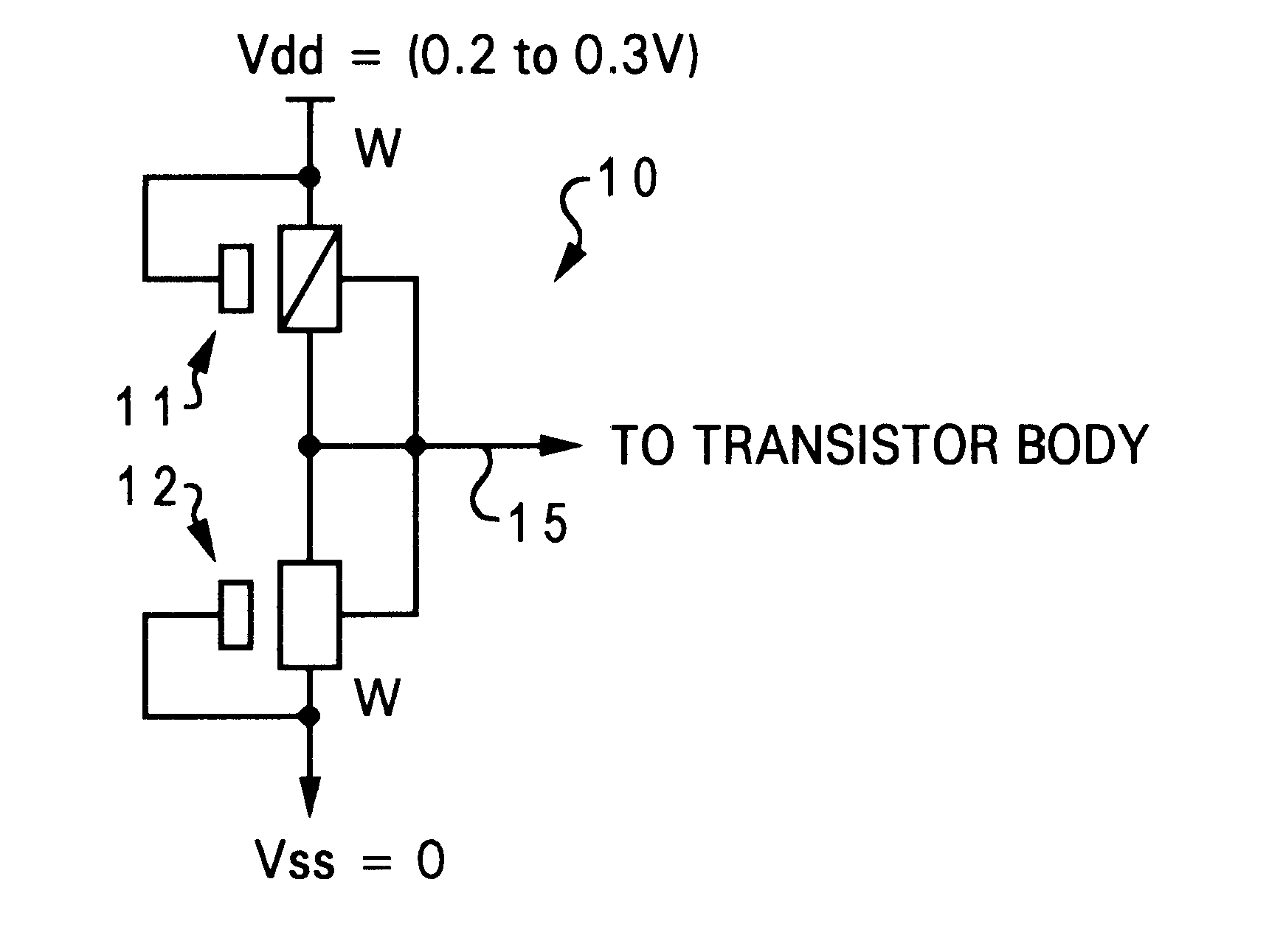
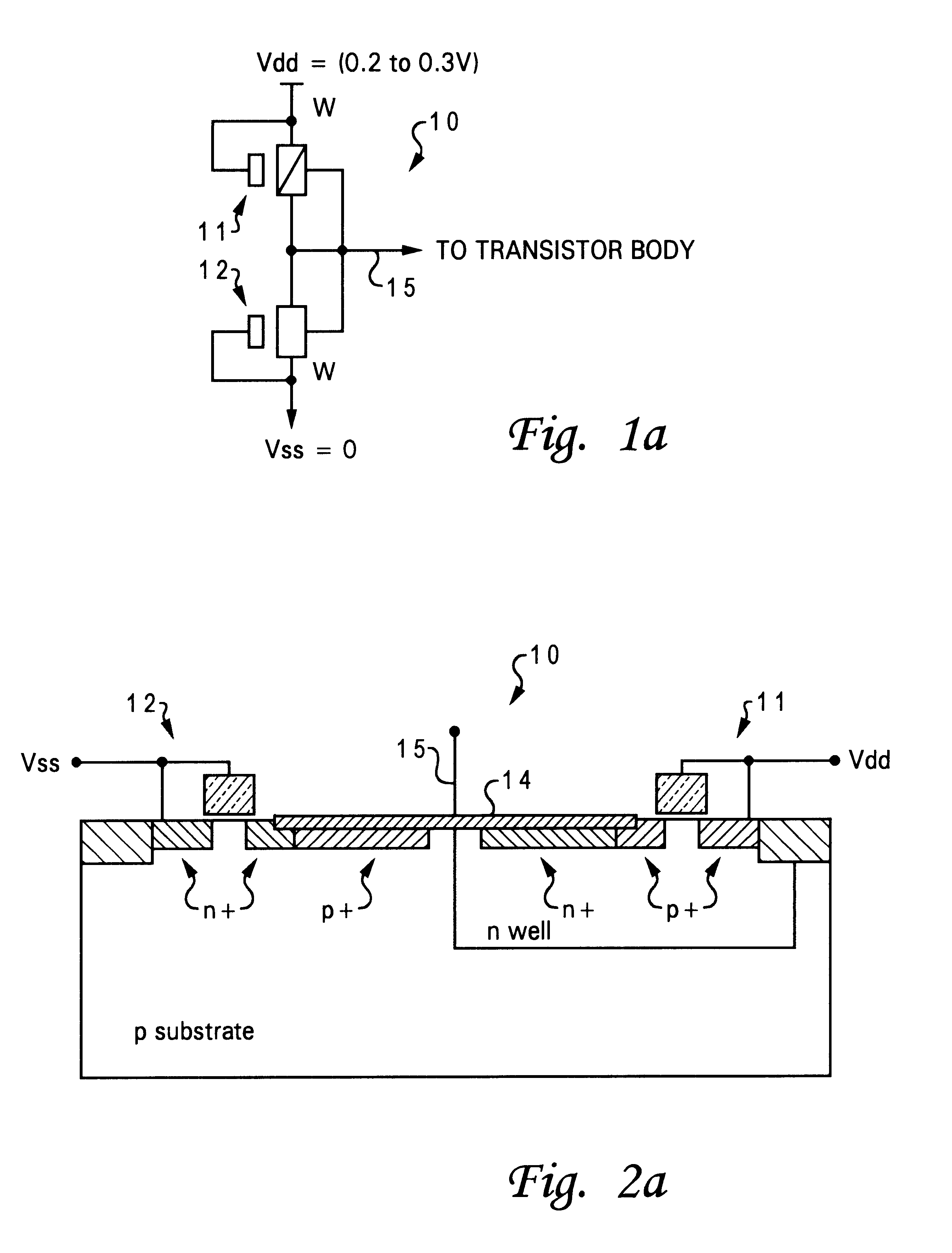
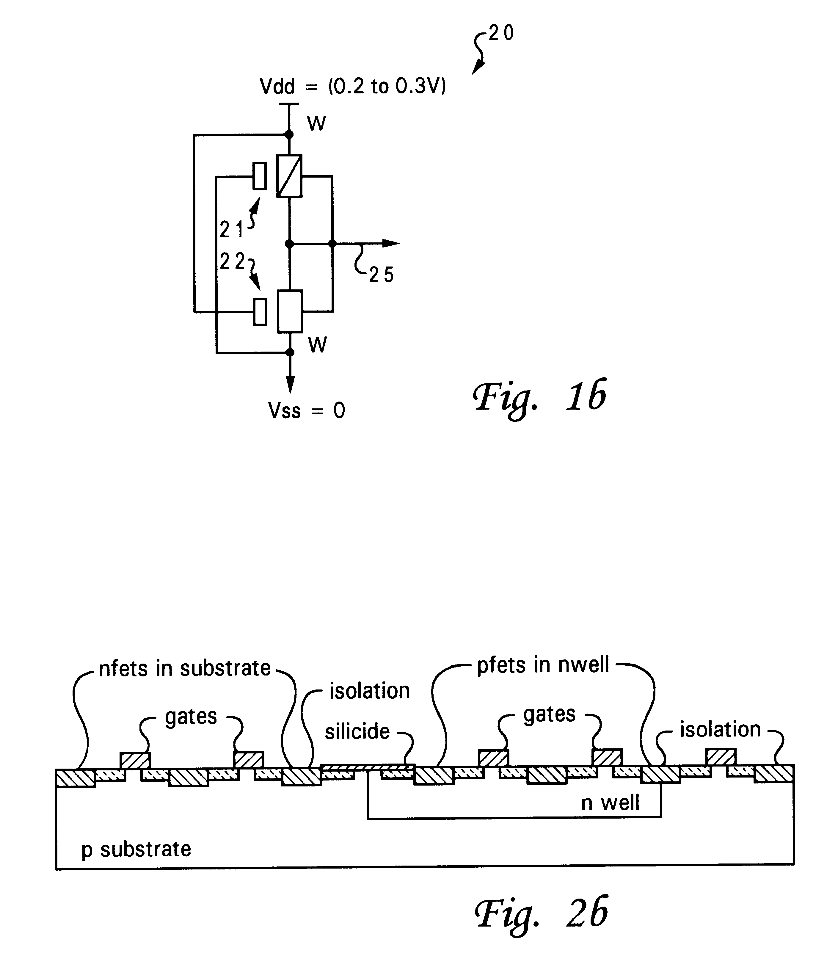
In accordance with a preferred embodiment of the present invention, a global body bias circuit is utilized to match the I.sub.off of N-channel and P-channel transistors with each other within a logic circuit by adjusting the bias of a global N-well and a substrate (or a global P-well). I.sub.off is the amount of current a transistor draws from its drain when its gate is tied to its source.

Referring now to the drawings and in particular to FIG. 1a, there is depicted a schematic diagram of a global body bias circuit having one output, in accordance with a preferred embodiment of the present invention. As shown, a global body bias circuit 10 includes a P-channel transistor 11 and an N-channel transistor 12 connected in series. The gate and source of P-channel transistor 11 are connected to a power supply V.sub.dd that provides a voltage ranging between 0.2 V-0.3 V. The gate and source of N-channel transistor 12 are connected to ground (or to a power supply V.sub.ss). The bodies and the...


PUM


Abstract

An apparatus for biasing ultra-low voltage logic circuits is disclosed. An integrated circuit device includes multiple transistors and a global body bias circuit. The global body bias circuit includes a first transistor and second transistors connected in series between a power supply and a second power supply or ground. The gate and source of the first transistor are connected to the first power supply. The gate and source of the second transistor are connected to the second power supply. The drains and bodies of the first and second transistors are connected together to form an output connected to the bodies of the other transistors within the integrated circuit device.

Description

1. Technical FieldThe present invention relates to integrated circuit devices in general, and in particular to an apparatus for biasing logic circuits within integrated circuit devices. Still more particularly, the present invention relates to an apparatus for biasing ultra-low voltage logic circuits within an integrated circuit device.2. Description of the Prior ArtMetal-oxide semiconductor field-effect transistors (MOSFETs) are commonly found in integrated circuit devices. A MOSFET includes a gate, a source, and a drain. The flow of charge carriers through a channel between the source and drain can be controlled by applying a voltage at the gate of a MOSFET. A depletion-mode MOSFET includes a doped or conducting channel under a gate even when no voltage is applied to the gate. An enhancement-mode MOSFET, in contrast, requires a gate-to-source bias voltage be applied in order to generate an inversion layer to serve as a conducting channel. Such bias voltage is known as a threshold ...

Claims


Application Information

Patent Timeline
Patent Type & Authority Patents(United States)
IPC IPC(8): G05F3/20G05F3/08H01L27/02H01L27/04H01L21/822H01L21/8238H01L27/092H03K19/094
CPCG05F3/205H01L27/0218
Inventor BRYANT, ANDRESCOTTRELL, PETER EDWINELLIS-MONAGHAN, JOHN JOSEPHKETCHEN, MARK B.NOWAK, EDWARD JOSEPH
Owner INT BUSINESS MASCH CORP
Why Eureka
Try Eureka