Ball attached zero insertion force socket

a zero-inserting force, ball-attached technology, applied in the direction of fixed connections, coupling device connections, electrical apparatus construction details, etc., can solve the problems of bga damage, electronic component damage, or both, and it is extremely difficult to reliably mount on a pcb without damaging the bga, electronic component or both, damage or even destruction of components

Inactive Publication Date: 2003-11-11
FCI AMERICAS TECH INC (US)
View PDF19 Cites 28 Cited by
  • Summary
  • Abstract
  • Description
  • Claims
  • Application Information

AI Technical Summary

Benefits of technology

The present invention is directed to a Zero Insertion Force (ZIF) socket and method for mechanically and electrically connecting an electronic component to a circuit substrate using a substantially ZIF socket. The ZIF socket includes a housing that defines a cavity for containing a middle plate that is selectively movable relative to the housing between a contact and a non-contact position The housing includes a plurality of apertures formed in a top surface and arranged to correspond with the contact terminals of an electronic component that can be mounted on the top surface of the ZIF socket. The middle plate has a plurality of apertures formed therein and arranged to substantially correspond with the contact terminals of the electronic component. The housing also includes a plurality of apertures formed in a bottom surface and arranged to correspond with the leads or pads of a circuit substrate. The circuit substrate may also include a plurality of holes formed in the circuit substrate for receiving mounting projections extending from the bottom surface of the ZIF socket housing. An electrically connective medium such as, for example, a solder medium, is disposed between and mechanically and electrically connects the ZIF socket housing to the circuit substrate.

Problems solved by technology

In multiple pin electronic components, especially those having a large number of pin terminals, such as microprocessor chips, the insertion force necessary to seat the electronic component in an associated socket can be considerable and can lead to difficulty in installation of the electronic component into the socket.
However, the very features of the hall grid array device which make it attractive as a device structure (e.g., closely grouped very small contacts arranged on a hidden face) make it extremely difficult to reliably mount on a PCB without damaging the BGA, the electronic component, or both.
The force required to remove the component from the socket, e.g., the force required to overcome the retention force of the connection, may also be of magnitude sufficient to cause damage or even destruction of the components.
The contact structures that receive the BGA contact balls typically attempt to provide sufficient electrical contact and retain the ability to articulate between the contact and non-contact position many times without jeopardizing its mechanical and electrical connection properties.
While beneficial in larger applications, traditional ZIF designs may not be preferred in high contact density applications.
Difficulties with known ZIF sockets include complexity and cost in high contact density situations, especially when miniaturization is required.
Further, the contact structures of ZIF sockets may not fit within a given footprint on the PCB.
When ZIF designs are used in high contact density applications, traditional ZIF sockets have not successfully maintained the contact between the electronic component and the PCB due to solder wicketing and difficulties with conventional soldering techniques.
The decreased amount of solder on the exterior of the ZIF socket often leads to a deteriorated electrical connection between the ZIF socket and the PCB.
Traditional ZIF sockets do not control the solder ball during reflow, and as a result, a poor connection is formed between the ZIF socket and the PCB.

Method used


Image

  • Ball attached zero insertion force socket
  • Ball attached zero insertion force socket
  • Ball attached zero insertion force socket

Examples


Embodiment Construction

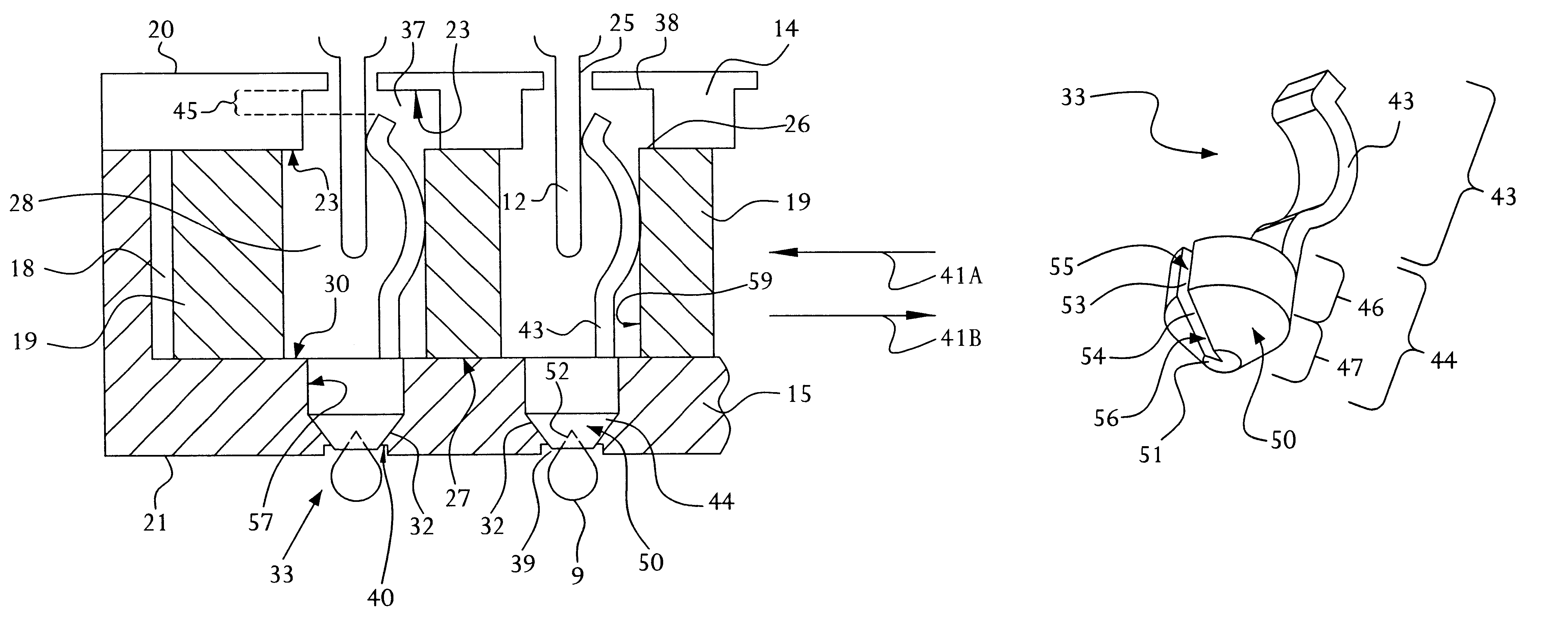
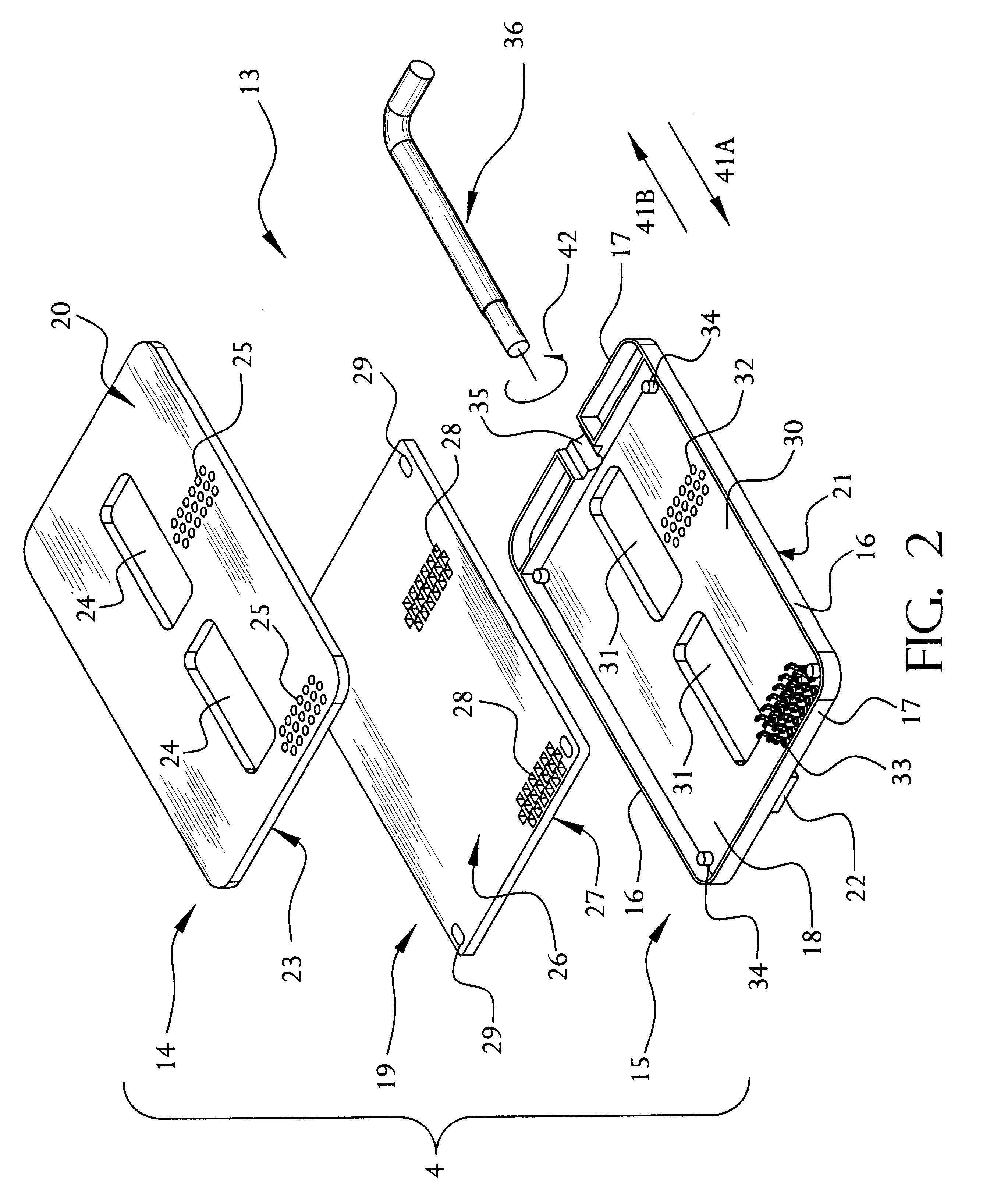
The present invention is directed to an apparatus, system, and method for connecting an electronic component to a circuit substrate and forming an electrical connection therebetween using a substantially zero insertion force (ZIF) socket. The present invention provides for an improved, more compliant, and more reliable connection between the ZIF socket and the circuit substrate and ultimately between the circuit substrate and the electronic component. The improved connection is formed by a press-fit contact assembly that includes a novel configuration for anchoring the contact assembly to the ZIF socket. The contact assembly is adapted to prevent and / or reduce solder wicketing during solder reflow and therefore creates a more reliable connection between the ZIF socket and the circuit substrate. In addition, the present invention provides for an improved configuration for attaching a solder medium, such as a solder ball, to the contact assembly. The present invention improves solder ...


PUM


Abstract

A system and method for mechanically and electrically connecting an electronic component and a circuit substrate using a Zero Insertion Force (ZIF) socket. The ZIF socket having a plurality of press-fit contact assemblies and a housing with middle plate that is selectively movable between a contact and non-contact position. Each contact assembly being secured to the ZIF socket housing by press-fitting the lower portion of the contact assembly such that each contact assembly is anchored to an aperture in the housing bottom by compressive force. The ZIF socket is mounted to the circuit substrate and the electronic component is mounted on to the ZIF socket. The contact assemblies of the ZIF socket are selectively movable between a contact and non-contact position. The press-fit contact assemblies form a seal to prevent solder wick-up.

Description

This invention relates generally to the field of electrical connectors, and particularly to a Zero Insertion Force (ZIF) socket for establishing a mechanical and electrical connection between an electronic component and a circuit substrate. More particularly, this invention relates to a BGA / LGA ZIF socket for connecting a processor package to a printed circuit board.BACKGROUND FOR THE INVENTIONElectronic components, such as integrated circuits, require a large number of electrical interconnections which occupy a small space in order to communicate properly with a circuit substrate. In order to provide electrical communication between the chip and external circuitry, circuit chips are usually contained within a housing or package which supports interconnection leads, pads, and the like on one or more of its external surfaces. The contact terminals may extend from a surface of the package in the form of, for example, a pin grid array (BGA), and a land grid array (LGA). A PGA includes ...

Claims


Application Information

Patent Timeline
Patent Type & Authority Patents(United States)
IPC IPC(8): H05K7/10H01R12/57H01R33/76H01R24/00
CPCH05K7/1007H01R12/85
Inventor WILSON, JOHN W.KELLER, REX W.ISSAK, GHYATH
Owner FCI AMERICAS TECH INC (US)
Why Eureka
Try Eureka