Thermally stable crystalline defect-free germanium bonded to silicon and silicon dioxide

a defect-free, germanium-based technology, applied in the direction of basic electric elements, electrical apparatus, semiconductor devices, etc., can solve the problems of germanium layer, high power consumption of electronic devices made using bulk si substrates, and the upper limit of the performance of electronic devices

Inactive Publication Date: 2003-11-11
INTEL CORP
View PDF4 Cites 73 Cited by
  • Summary
  • Abstract
  • Description
  • Claims
  • Application Information

AI Technical Summary

Problems solved by technology

Additionally, electronic devices made using bulk Si substrates require high power consumption due to current substrate leakage, especially for high performance devices.
The lower mobility and the current substrate leakage problem in using bulk Si for substrate set upper limits on the performance of the electronic devices with regard to material and power dissipation aspects.
Defects in the germanium layer in a Si--Ge alloy are undesirable since they reduce Ge's carrier mobility, and adversely affect the electronic quality and performance reliability of various electronic devices.
And, bonding of a Ge wafer directly a Si wafer have not been successful because such bonding suffers from other defects such as thermally induced slip, bonding voids, unstable or weak interface and crystalline defect.

Method used


Image

  • Thermally stable crystalline defect-free germanium bonded to silicon and silicon dioxide
  • Thermally stable crystalline defect-free germanium bonded to silicon and silicon dioxide
  • Thermally stable crystalline defect-free germanium bonded to silicon and silicon dioxide

Examples


Embodiment Construction

In the following description, for purposes of explanation, numerous specific details are set forth. It will be evident, however, to one skilled in the art that the embodiments of present invention may be practiced without these specific details. In other instances, specific apparatus structures and methods have not been described so as not to obscure the present invention.

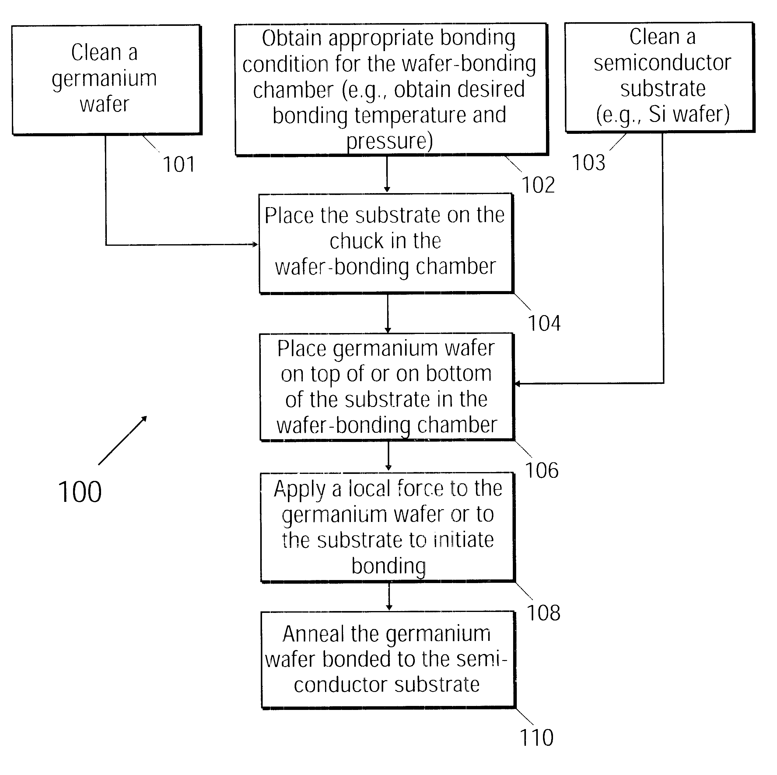
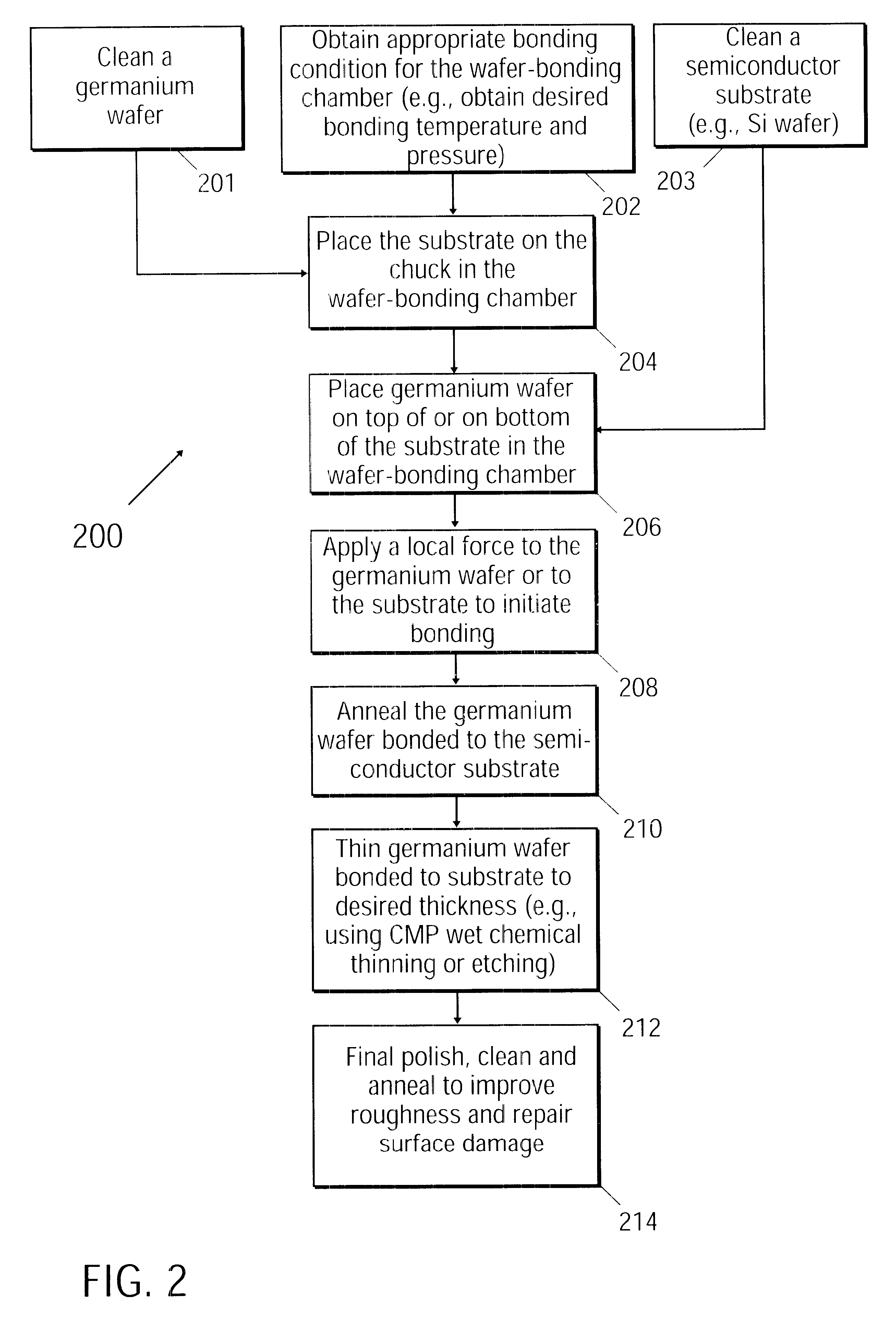
Defect-free germanium (Ge) is a key issue affecting the integration of silicon substrates having Ge films for silicon integrated circuits in electronic, optoelectronic applications and other suitable electronic devices, for example, in making transistors and detectors. The embodiments of the present invention direct to methods of bonding a Ge wafer directly to a semiconductor wafer such as silicon (Si) wafer or silicon containing wafer that results in substantially defect-free wafer pair. The term wafer pair refers to the Ge wafer bonded to the semiconductor wafer mentioned above. To create the substantially defect...


PUM


Abstract

A wafer pair comprising a substantially defect-free germanium wafer and methods of making the same. The wafer pair comprises the substantially defect-free germanium wafer directly bonded to a silicon wafer. The method of making the wafer pair comprises placing the silicon wafer in a wafer-bonding chamber, placing the germanium wafer on top or on bottom of the silicon wafer, and applying a local force to either the germanium wafer or to the silicon wafer to initiate bonding of the germanium wafer to the silicon wafer. The bonding occurs under a temperature ranging from about 23° C. to about 600° C. and under a vacuum condition inside a wafer-bonding chamber.

Description

1. FieldThe present invention relates to a substantially defect-free germanium wafer for use in a semiconductor device and in particular, to semiconductor devices comprising a substantially defect-free germanium wafer bonded to a silicon containing substrate without the need of an intermediate layer. The present invention further concerns the methods for making and using such devices.2. Discussion of Related ArtThere is increasing interest in using silicon-germanium (Si--Ge) alloy as a material for microelectronic and optoelectronic device applications. Germanium (Ge) is known to have high carrier mobility (e.g., high hole and electron mobility) and optical absorption as compared to silicon (Si). This is one reason why Ge is useful for devices that require enhanced performance and / or high quantum efficiency. Examples of devices that would benefit from the use of a Ge film include metal-oxide-semiconductor (MOS) transistors, optical detectors, and other optoelectronic devices, to nam...

Claims


Application Information

Patent Timeline
Patent Type & Authority Patents(United States)
IPC IPC(8): H01L21/70H01L21/285H01L21/18H01L21/02H01L29/45H01L21/762H01L29/02H01L29/165H01L29/40
CPCH01L21/187H01L21/28512H01L21/76256H01L29/45H01L21/76283H01L29/165H01L21/76275
Inventor SHAHEEN, MOHAMAD A.JIN, BEENYIHCHAU, ROBERT S.
Owner INTEL CORP
Why Eureka
Try Eureka