

Semiconductor pressure sensor having strain gauge and circuit portion on semiconductor substrate
a technology of semiconductor substrate and strain gauge, which is applied in the direction of fluid pressure measurement, acceleration measurement using interia forces, microstructured devices, etc., can solve the problems of sensor characteristics deteriorating, sensor characteristics being adversely affected by locos film
- Summary
- Abstract
- Description
- Claims
- Application Information
AI Technical Summary
Problems solved by technology
Method used
Image

Examples
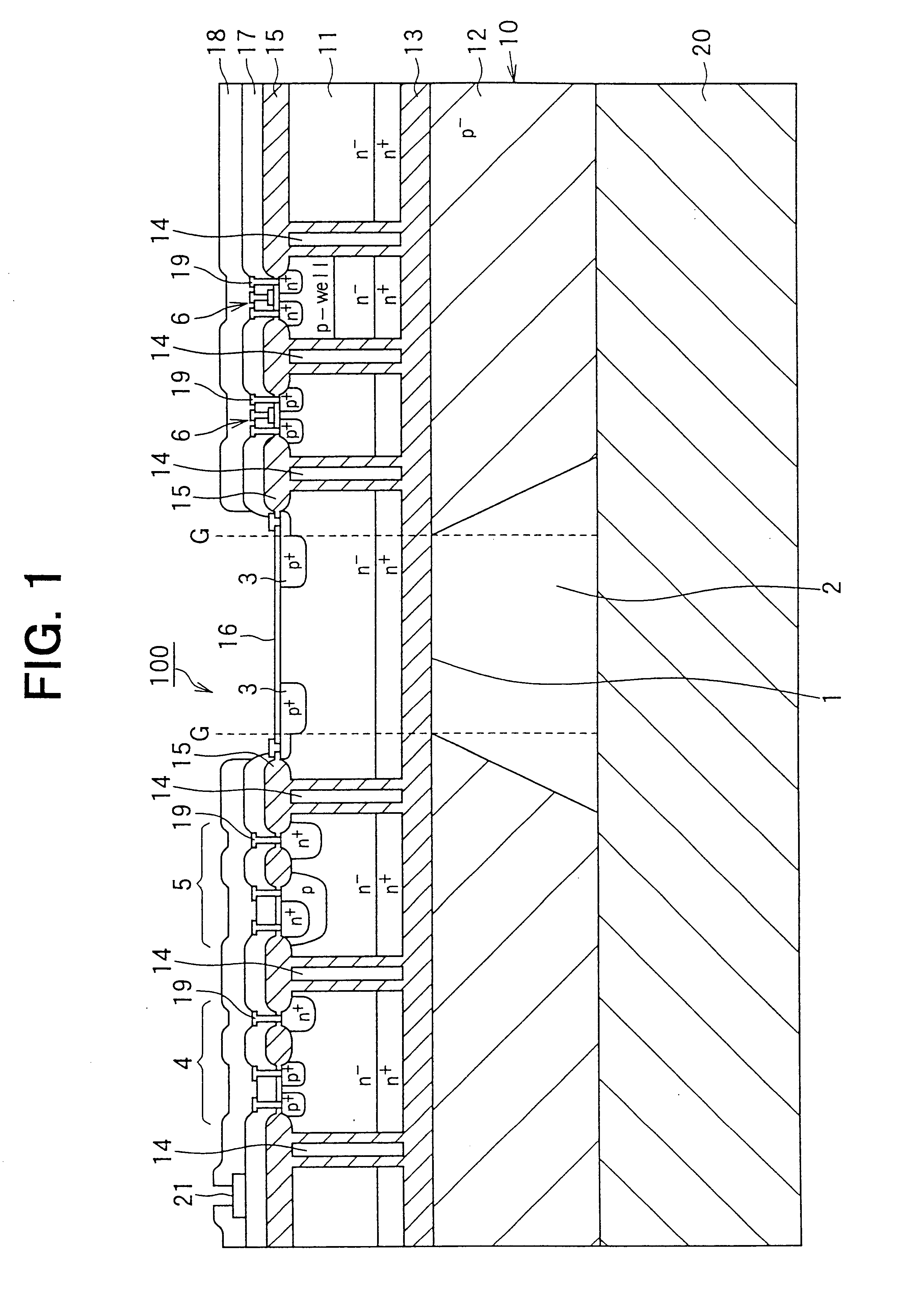
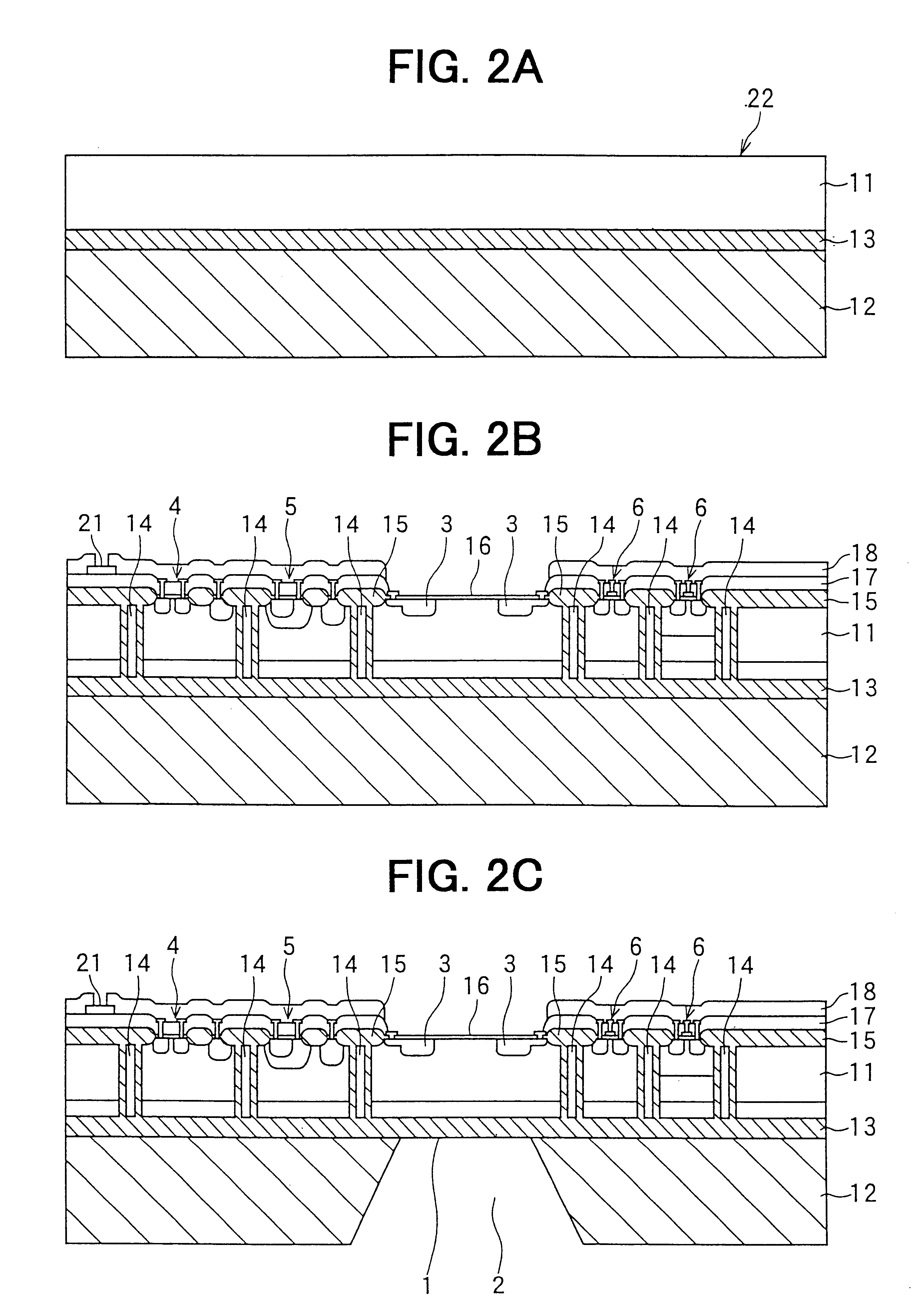
first embodiment
In the first embodiment, the second silicon substrate 12 is entirely removed in the thickness direction to provide the recess portion 2, so that the first silicon substrate 11 and the embedded oxide film 13 remain corresponding to the recess portion 2, and form the diaphragm portion 1. However, the embedded oxide film 13 may also be entirely removed in the thickness direction so that the diaphragm portion 1 can be composed only of the first silicon substrate 11. Otherwise, the second silicon substrate 12 may not be entirely removed in the thickness direction so that the diaphragm portion 1 can be composed of the first silicon substrate 11, the embedded oxide film 13 and the partially remaining second silicon substrate 12.
Strain gauges (gauge diffused resistors) 3 for generating electric signals in accordance with deformation of the diaphragm portion 1 are formed on the diaphragm portion 1 of the first silicon substrate 11 so as to form a Wheatstone bridge circuit. A circuit portion ...
second embodiment
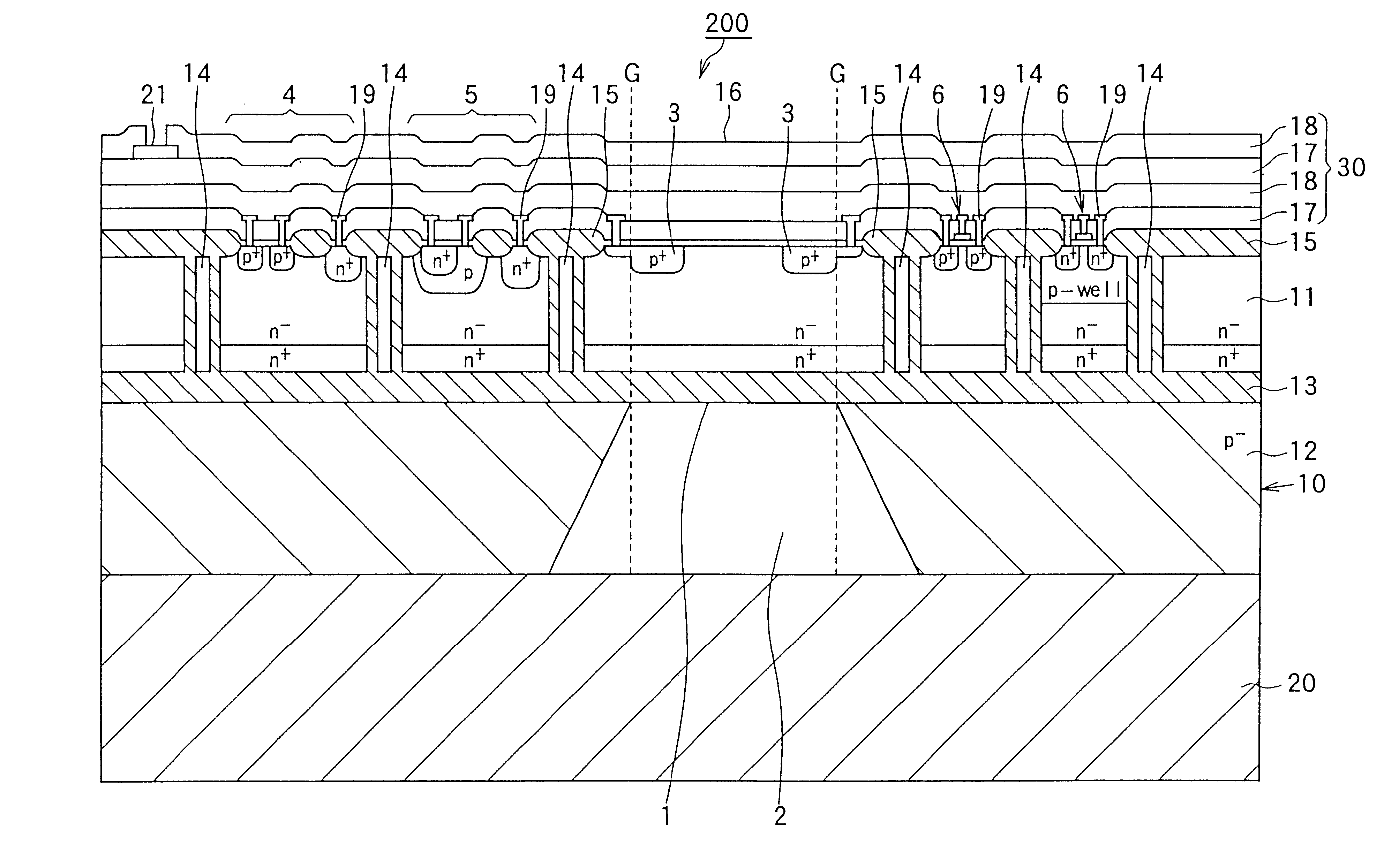
The main object of the second embodiment is to improve an environment resistance in a semiconductor pressure sensor 200 in which a diaphragm portion, digital circuit elements and analog circuit elements are integrated on a single semiconductor chip. For example, the semiconductor pressure sensor 200 according to the second embodiment can be preferably used as a vehicle intake-pressure sensor or the like, which is liable to be disclosed to contaminants in a severe environment. Hereinafter, the second embodiment will be described with reference to FIG. 7 mainly on points different from the first embodiment.
The semiconductor pressure sensor 200 according to the second embodiment is mainly characterized in as follows. That is, the diaphragm portion 1 and the circuit portion are coated and protected by a protection film 30 formed on the main surface of the semiconductor substrate 10 at the side of the first silicon substrate 11. Further, the protection film 30 includes at least two SiN s...
third embodiment
As shown in FIG. 8, a semiconductor pressure sensor 300 according to a third embodiment has substantially the same structure as that shown in FIG. 1 excepting the recess portion 2 provided in the second silicon substrate 12. A recess portion 23 shown in FIG. 8 is provided so as not to reach the embedded oxide film 13. In the third embodiment, the same operational effects as those in the first embodiment can be also obtained.
In the above-described embodiments, it is feared that the strain gauges 3 are adversely affected by stress of the trenches 14. Therefore, it is preferable that the trenches are provided outside the periphery of the diaphragm portion 1.
Here, relationships between the position of the trench 14 and sensitivity and between the position of the trench 14 and offset voltage were studied by using a model shown in FIGS. 9A and 9B.
In the model, the trench 14 is provided by vertically etching silicon, and the sidewalls of the trench 14 are oxidized. Thereafter, polysilicon ...
PUM
| Property | Measurement | Unit |
|---|---|---|
| distance | aaaaa | aaaaa |
| thickness | aaaaa | aaaaa |
| thickness | aaaaa | aaaaa |
Abstract
Description
Claims
Application Information