Method for manufacturing high-voltage lateral dual-diffusion N-channel metal oxide semiconductor (NMOS) based on standard complementary metal-oxide-semiconductor transistor (CMOS) process

A technology of lateral double-diffusion and manufacturing method, which is applied in the field of high-voltage lateral double-diffusion NMOS manufacturing. It can solve the problems of lowering the requirements of photolithographic alignment, difficult manufacturing process, and integration, and achieves short channel length and optimal current drive. and the effect of conduction capability

Active Publication Date: 2011-09-14
ADVANCED SEMICON MFG CO LTD
View PDF3 Cites 16 Cited by
  • Summary
  • Abstract
  • Description
  • Claims
  • Application Information

AI Technical Summary

Problems solved by technology

Compared with traditional high-voltage MOSFET devices such as DECMOS, the power device of this lateral diffusion structure can obtain a shorter self-aligned channel size to reduce the requirement of photolithography alignment level, and because the channel has a higher concentration gradient , to prevent the occurrence of punch-through and improve the driving capability, but the biggest disadvantage of traditional LDNMOS is that its manufacturing process is difficult to integrate w

Method used


Image

  • Method for manufacturing high-voltage lateral dual-diffusion N-channel metal oxide semiconductor (NMOS) based on standard complementary metal-oxide-semiconductor transistor (CMOS) process
  • Method for manufacturing high-voltage lateral dual-diffusion N-channel metal oxide semiconductor (NMOS) based on standard complementary metal-oxide-semiconductor transistor (CMOS) process
  • Method for manufacturing high-voltage lateral dual-diffusion N-channel metal oxide semiconductor (NMOS) based on standard complementary metal-oxide-semiconductor transistor (CMOS) process

Examples


Embodiment Construction

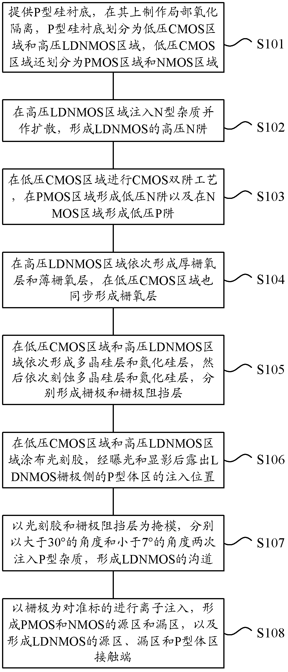
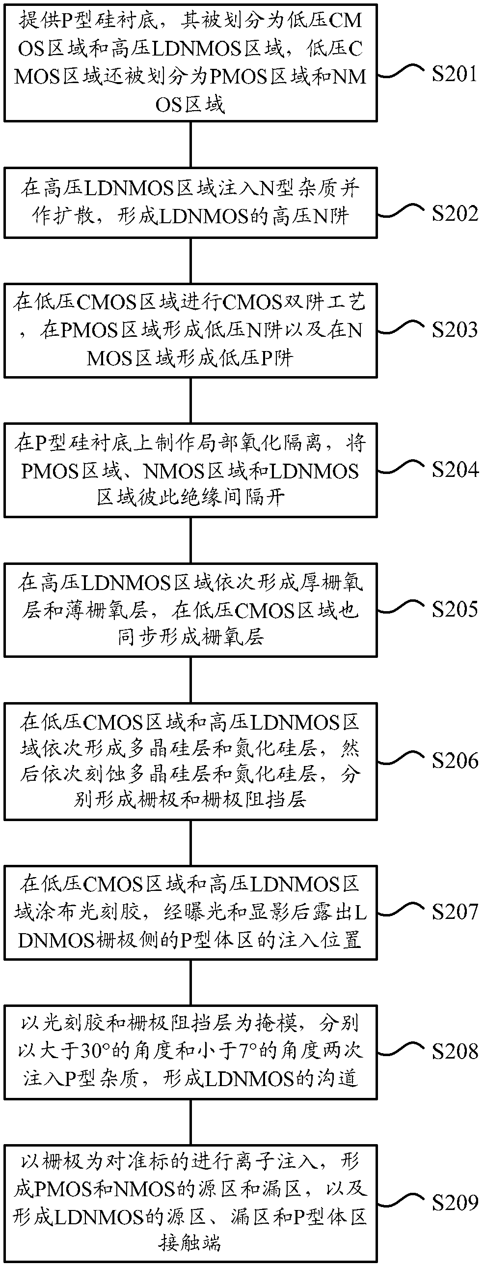
[0038] The present invention will be further described below in conjunction with specific embodiments and accompanying drawings, but the protection scope of the present invention should not be limited thereby.

[0039] figure 1 It is a schematic flowchart of a method for fabricating a high-voltage lateral double-diffusion NMOS based on a standard CMOS process according to an embodiment of the present invention. As shown in the figure, the fabrication method of the high-voltage lateral double-diffused NMOS (LDNMOS) may include:

[0040] Executing step S101, providing a P-type silicon substrate on which local oxidation isolation is made, the P-type silicon substrate is divided into a low-voltage CMOS region and a high-voltage LDNMOS region, and the low-voltage CMOS region is further divided into a PMOS region and an NMOS region;

[0041] Executing step S102, implanting and diffusing N-type impurities in the high-voltage LDNMOS region to form a high-voltage N well of the LDNMOS;...


PUM

PropertyMeasurementUnit
Thicknessaaaaaaaaaa
Thicknessaaaaaaaaaa

Abstract

The invention provides a method for manufacturing a high-voltage lateral dual-diffusion N-channel metal oxide semiconductor (NMOS) based on a standard complementary metal-oxide-semiconductor transistor (CMOS) process. The method comprises the following steps of: providing a P type silicon substrate, manufacturing local oxidation of silicon (LOCOS) on the P type silicon substrate, and dividing theLOCOS into a low-voltage CMOS area and a high-voltage lateral diffused N-channel metal oxide semiconductor (LDNMOS) area; injecting phosphor into the LDNMOS area and diffusing the phosphor to form a high-voltage N well; performing a two-well process in the CMOS area to form a low-voltage N well and a low-voltage P well; sequentially forming a thick gate oxide layer and a thin gate oxide layer in the LDNMOS area; sequentially forming a polysilicon layer and a silicon nitride layer and sequentially etching the polysilicon layer and the silicon nitride layer to form a grid electrode and a buffering layer respectively; coating a photoresist, and exposing the injection position of a P type area of the LDNMOS area after exposing and development; injecting P type ions for two times at the anglesof more than 30 degrees and less than 7 degrees respectively to form channels of an LDNMOS, wherein the photoresist and the buffering layer serve as masks; and forming source areas and drain areas ofa P-channel metal oxide semiconductor (PMOS) and an NMOS, and contact ends of a source area, a drain area and a P type area of the LDNMOS by taking the grid electrode as an alignment mark. Because a large-angle injection process is used for forming the channels after the grid electrode is formed, a long-time high-temperature heating process is not required and the process is compatible.

Description

technical field [0001] The present invention relates to the technical field of semiconductor manufacturing, in particular, the present invention relates to a high-voltage lateral double-diffused NMOS (Lateral Double Diffused NMOS, LDNMOS for short) manufacturing method based on a standard CMOS process. Background technique [0002] High-voltage MOSFET drive devices and their modules (12V~30V LDNMOS, DDDMOS, DECMOS, etc.) are widely used in LED backlight drive, motor drive, and chip control, and are a hot research field in recent years. [0003] Among them, a power device with a lateral diffusion structure (Lateral Diffused MOSFET, LDMOS for short) is one of the most popular devices. The traditional high lateral double-diffusion NMOS (LDNMOS) uses the principle of simultaneous implantation of boron (P) and arsenic (As) ions, and the principle that boron diffuses faster than arsenic in the high-temperature and long-term thermal process to form a fixed-length self-aligned P-ty...

Claims


Application Information

Patent Timeline
IPC IPC(8): H01L21/336H01L21/266
Inventor 刘建华林威
Owner ADVANCED SEMICON MFG CO LTD
Why Eureka
Try Eureka