Flash memory process with high voltage LDMOS embedded

a technology of flash memory and laterally diffused metal oxide, which is applied in the direction of semiconductor devices, electrical equipment, basic electric elements, etc., can solve the problems of difficulty in simultaneously fabricating the lower power devices with the higher power devices, and the early generation of ldmos can only work at voltages up to about 14v, so as to achieve less forming steps, lower production cost, and higher performance

Inactive Publication Date: 2007-10-16
TAIWAN SEMICON MFG CO LTD
View PDF10 Cites 16 Cited by
  • Summary
  • Abstract
  • Description
  • Claims
  • Application Information

AI Technical Summary

Benefits of technology

[0007]The preferred embodiment of the present invention embeds the forming of flash cells and the forming of peripheral devices, including high voltage laterally diffused MOS (HV-LDMOS) and low-voltage devices. Various forming steps are combined so that production cost is lowered.
[0010]The advantages of the present invention include but are not limited to: lower production cost due to less forming steps; higher performance due to integrated low voltage and high voltage devices; and higher breakdown voltage of the LDMOS. The breakdown voltage of the HV-LDMOS made by the preferred embodiment of the present invention is above 15V, and the breakdown voltage may be adjusted in a wide range based on the requirement without major changes to the forming process.

Problems solved by technology

However, the early generation of the LDMOS can only work at voltages up to about 14V.
A problem with this technique is that it can be quite difficult to simultaneously fabricate the lower power devices with the higher power devices.

Method used


Image

  • Flash memory process with high voltage LDMOS embedded
  • Flash memory process with high voltage LDMOS embedded
  • Flash memory process with high voltage LDMOS embedded

Examples


Embodiment Construction

[0018]The making and using of the presently preferred embodiments are discussed in detail below. It should be appreciated, however, that the present invention provides many applicable inventive concepts that can be embodied in a wide variety of specific contexts. The specific embodiments discussed are merely illustrative of specific ways to make and use the invention, and do not limit the scope of the invention.

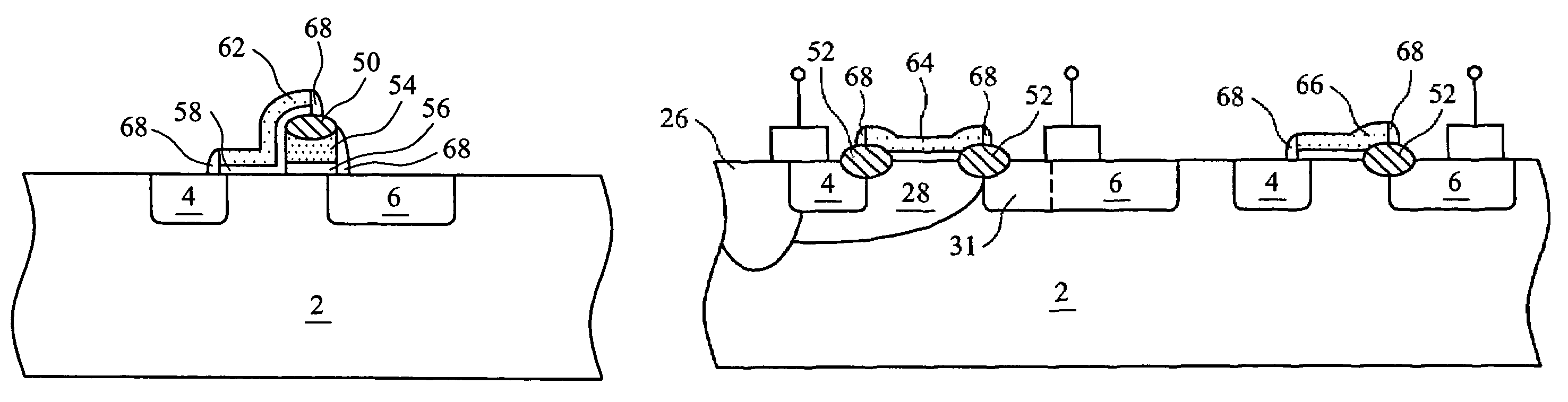
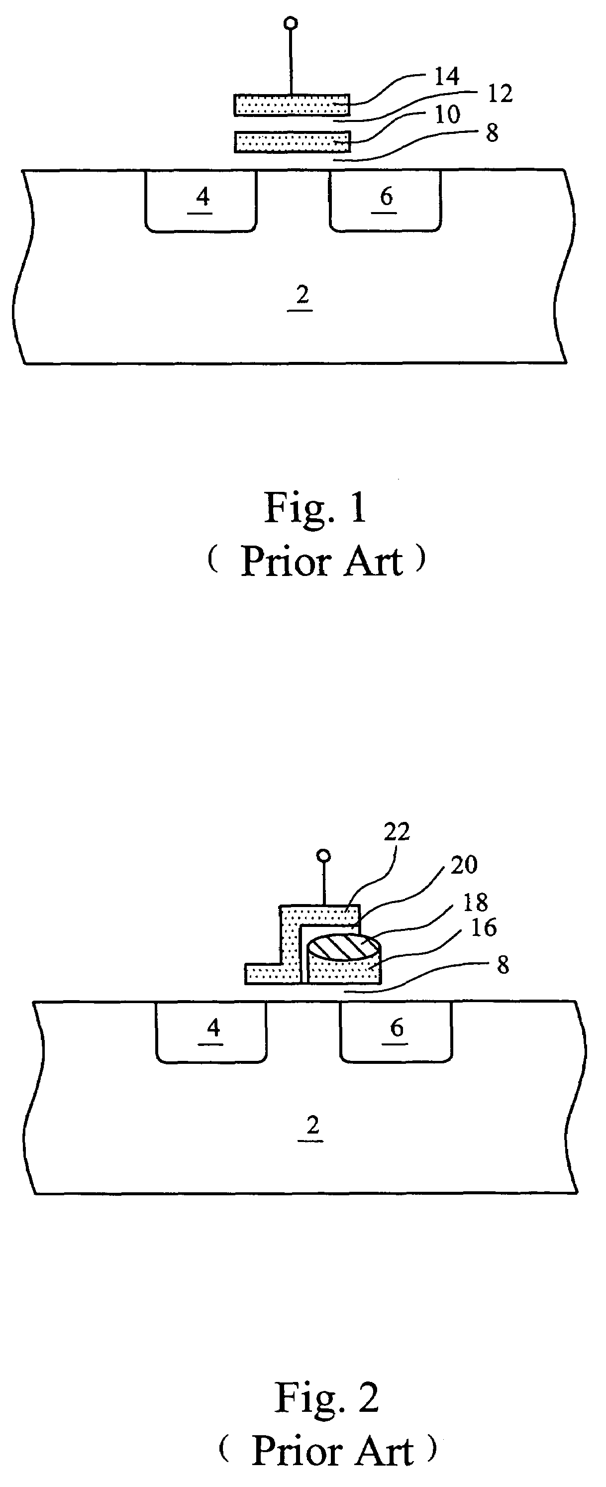
[0019]The preferred embodiments present a novel method of integrating the manufacturing of flash cells and higher voltage peripheral devices, such as high voltage laterally diffused MOS (HV-LDMOS) devices. The preferred embodiments combine various masks and forming steps by forming various elements of flash cells and HV-LDMOS devices at the same time. The flash cell could include stacked gate flash type or split gate flash type. The following method uses the split gate as an embodiment to illustrate the present invention.

[0020]The preferred embodiments are illustrated in FIGS...


PUM


Abstract

A method of embedding the forming of peripheral devices such as HV-LDMOS into the forming of flash memory is presented. A layered structure is formed with a first insulating layer formed on a substrate, and a poly silicon formed on the first insulating layer in the flash memory region. A mask layer is formed. Openings are formed in the flash memory region in the peripheral region. A local oxidation of silicon (LOCOS) is performed to form thick oxides on poly silicon, and a field oxide on silicon substrate respectively. The mask layer is removed. A control gate and a control gate oxide are formed on the thick oxide and the poly silicon. A gate electrode is formed with at least one end residing on a field oxide so that the resulting HV-LDMOS has a high breakdown voltage. Spacers and a source / drain of the flash cells and HV-LDMOSs are then formed.

Description

TECHNICAL FIELD[0001]This invention relates generally to semiconductor devices, and more specifically to the manufacturing of flash memory and high voltage laterally diffused metal-oxide semiconductor devices.BACKGROUND[0002]Flash memory has become popular recently. A typical flash memory comprises a memory array having a large number of memory cells arranged in blocks. Each of the memory cells is fabricated as a field-effect transistor having a control gate and a floating gate. The floating gate is capable of holding a charge and is separated from source and drain regions contained in a substrate by a layer of thin oxide. Each of the memory cells can be electrically charged by injecting electrons from the drain region through the oxide layer onto the floating gate. The charge can be removed from the floating gate by tunneling the electrons to the source through the oxide layer during an erase operation. Thus the data in a memory cell is determined by the presence or absence of a ch...

Claims


Application Information

Patent Timeline
Patent Type & Authority Patents(United States)
IPC IPC(8): H01L21/8247
CPCH01L21/28273H01L27/11521H01L27/115H01L29/40114H10B69/00H10B41/30
Inventor LU, HSIANG-TAIKUO, CHENG-HSIUNGWANG, CHIN-HUANG
Owner TAIWAN SEMICON MFG CO LTD
Why Eureka
Try Eureka