

Semiconductor device and method for manufacturing the same
a semiconductor and semiconductor technology, applied in semiconductor devices, semiconductor/solid-state device details, electrical apparatus, etc., can solve the problems of inability to the increase of drain-to-source breakdown voltage, and achieve the reduction of on-resistance, increase the drain-to-source breakdown voltage, and reduce the effect of on-resistan
- Summary
- Abstract
- Description
- Claims
- Application Information
AI Technical Summary
Benefits of technology
Problems solved by technology
Method used
Image

Examples
first embodiment
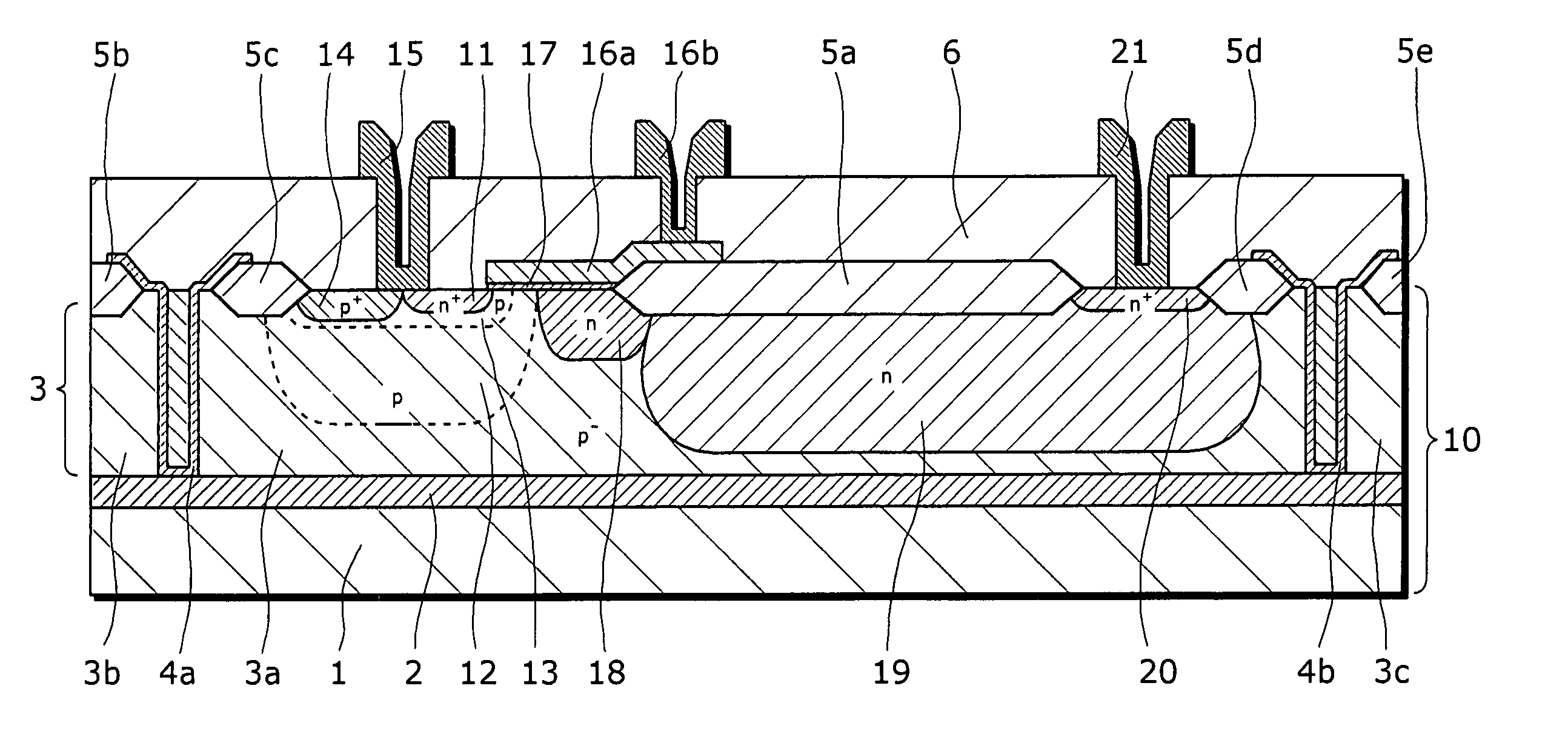
[0065]FIG. 3 is a cross-sectional view showing a structure of an N channel MOS transistor according to a first embodiment of the present invention.
[0066] As shown in FIG. 3, the MOS transistor according to the first embodiment has an offset structure, and is composed of: a SOI substrate 10; LOCOS films 5a to 5e having respective thickness of more than 300 nm, for example, about 420 nm that are formed on the SOI substrate 10 by a LOCOS method; a source electrode 15, a drain electrode 21 and a gate lead-out electrode 16b that are made of metal; a gate electrode 16a that is made of polysilicon; a gate oxide film 17 that is made of a silicon dioxide film having a thickness of about 10 nm to 20 nm which is formed by a thermal oxidation process; and an interlayer insulating film 6 that covers the SOI substrate 10.
[0067] The SOI substrate 10 is made up of: a supporting substrate (silicon substrate) 1; a buried oxide film 2 having a thickness of about 1 μm to 3 μm that is formed on the su...
second embodiment
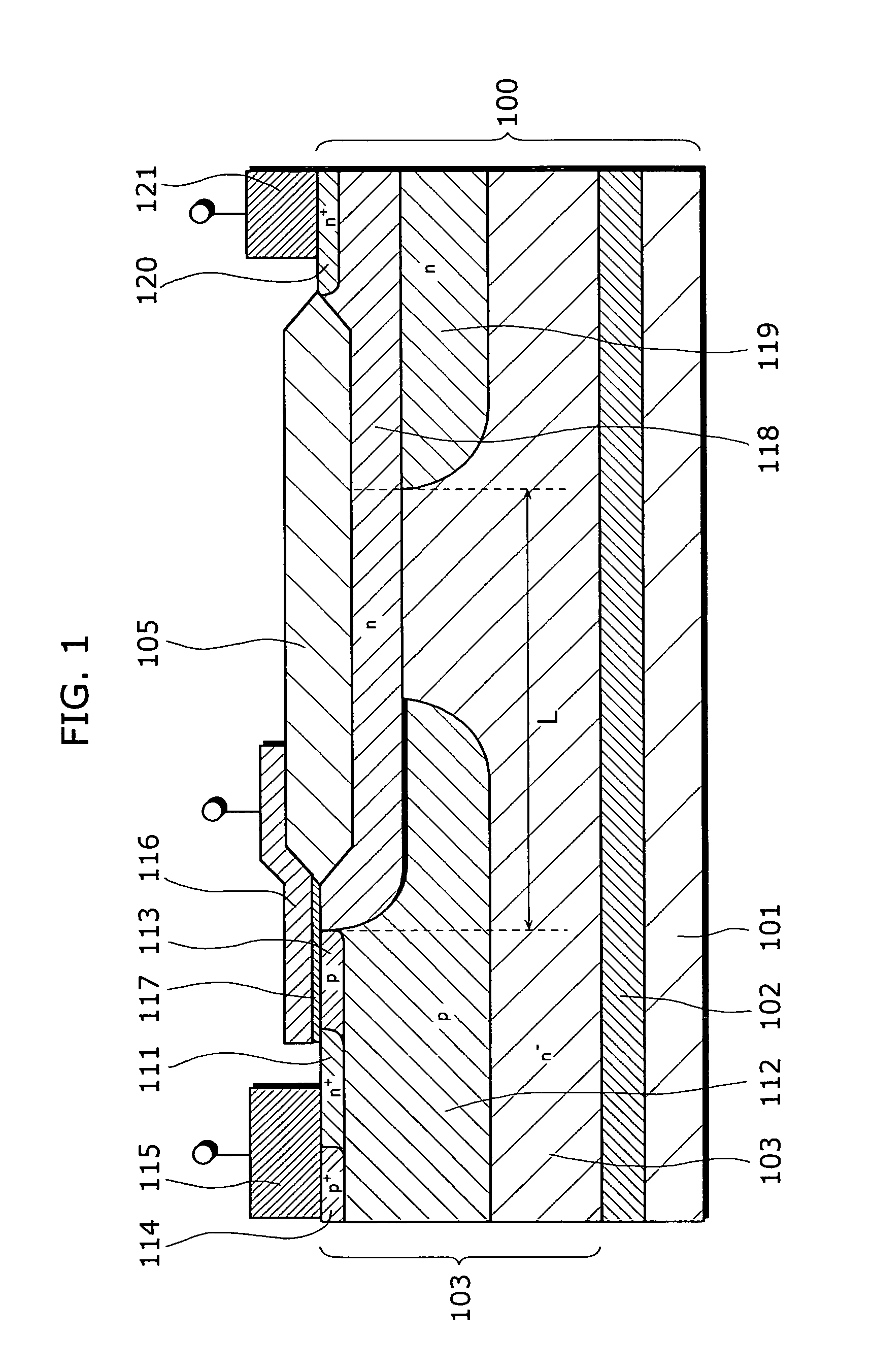
[0097]FIG. 8 is a cross-sectional view showing a structure of an N channel MOS transistor according to a second embodiment of the present invention. Note that dashed lines in FIG. 8 show a potential distribution in the MOS transistor when a gate electrode and a source electrode are set to 0 V and a positive high voltage is applied to a drain electrode.
[0098] As shown in FIG. 8, the MOS transistor according to the second embodiment differs from the MOS transistor according to the first embodiment in that it has a P type impurity region 23 of a high concentration immediately under the N type drain buffer region 18.
[0099] Next, the following describes a method for manufacturing the MOS transistor having the above structure.
[0100]FIGS. 9A to 9D and 10A to 10D are cross-sectional sequential views showing processes in the method for manufacturing the MOS transistor.
[0101] First, as shown in FIGS. 9A and 9B, a resist film 7 for forming the P type body region 12 is formed on the semicon...
PUM
 Abstract
Description
Claims
Application Information