Method of integrating volatile and non-volatile memory cells on the same substrate and a semiconductor memory device thereof

a memory cell and volatile technology, applied in the direction of semiconductor devices, electrical equipment, basic electric elements, etc., can solve the problems of power consumption of flash memory, inability to save data during power down, and significant factor in battery life, so as to improve communication, reduce manufacturing costs, and simplify the process

Inactive Publication Date: 2003-12-30
GOOGLE LLC
View PDF13 Cites 116 Cited by
  • Summary
  • Abstract
  • Description
  • Claims
  • Application Information

AI Technical Summary

Benefits of technology

It is another object of the present invention to provide a method of merging volatile and non-volatile memory devices in a single chip through a simplified process.
It is still another object of the present invention to provide a method of fabricating volatile and non-volatile memory devices and support devices on a single chip using a process having minimized steps.
It is further object of the present invention to provide a semiconductor memory device with high integration density by integrating DRAM and flash memory devices and support devices in a single chip.
A semiconductor memory device having structure of merged DRAM and flash memory devices also improves communication between memory and a central processing unit as well as communication between the DRAM and flash memory devices. Also, the existing DRAM built-in-self-test (BIST) technique allows DRAM to be tested at a high-speed without accessing all the internal nodes. Thus, the merged structure of DRAM and flash memory devices would be a low-cost solution of the problems in the conventional memory devices.
In the method of integrating the semiconductor memory device of the present invention, the process of integrating flash memory and DRAM devices may share as many process steps as possible so that the process is simplified and the manufacturing cost is reduced.

Problems solved by technology

In such electronic systems, power consumption is an important factor determining the battery lifetime.
Also, the data read power consumption in the flash memory is about 1.6 times as large as that of the DRAM.
Drawbacks in the DRAM devices include incapability of saving data during power is down.
This refresh process not only consumes power but also interrupts the availability of the data when the system requests.
Semiconductor memory devices having the DRAM and flash memory devices using the multi-chip packages have drawbacks such as high manufacturing cost, degradation of the system performance, decrease in the integration density, and so on.
Semiconductor memory devices fabricated using the conventional multi-chip approach are degraded in their performance due to narrow bandwidth.
This is because stand-alone chips in a multi-chip package have limitation in data input / output.
Thus, such a limitation restricts the number of data bandwidth.

Method used


Image

  • Method of integrating volatile and non-volatile memory cells on the same substrate and a semiconductor memory device thereof
  • Method of integrating volatile and non-volatile memory cells on the same substrate and a semiconductor memory device thereof
  • Method of integrating volatile and non-volatile memory cells on the same substrate and a semiconductor memory device thereof

Examples


Embodiment Construction

Detailed illustrative embodiments of the present invention are disclosed herein. However, specific structural and functional details disclosed herein are merely representative for purposes of describing preferred embodiments of the present invention.

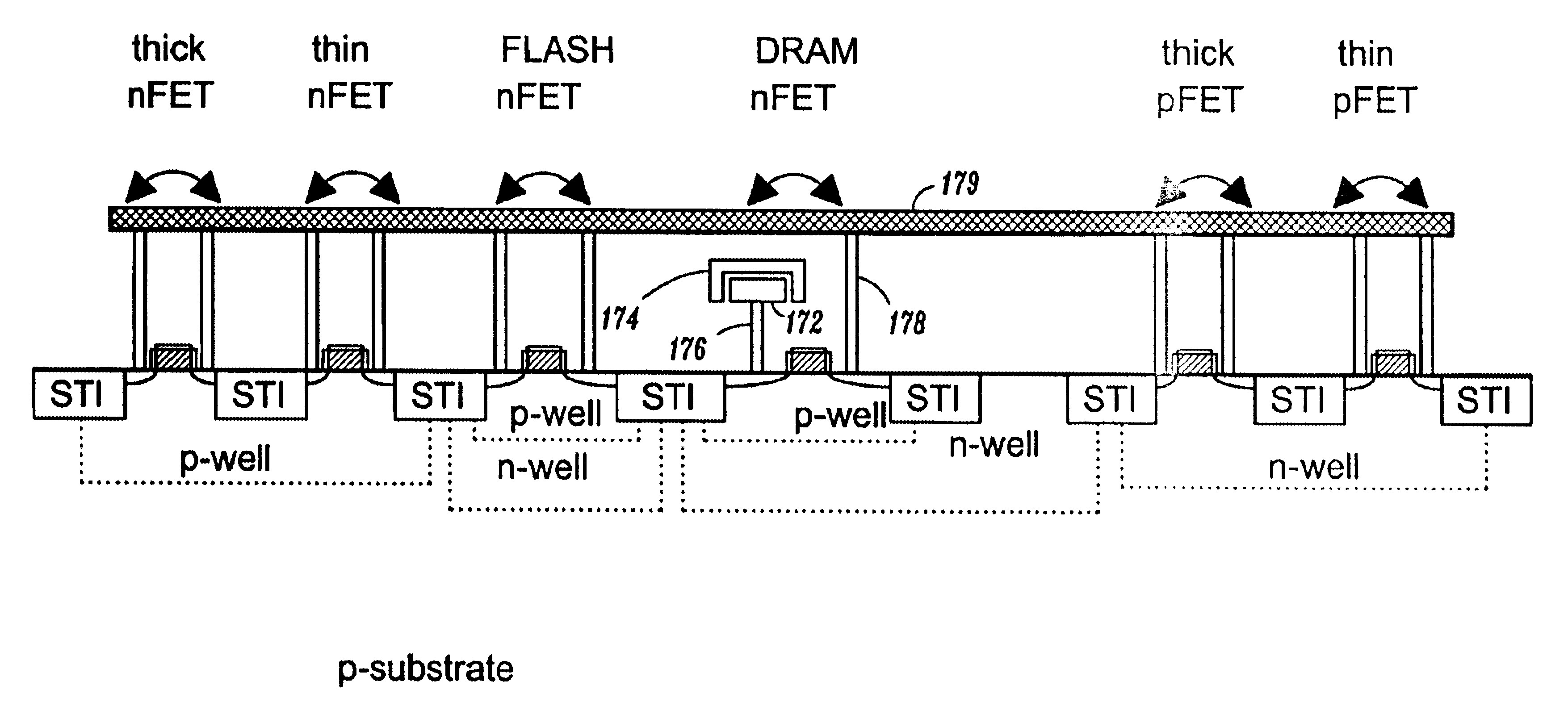
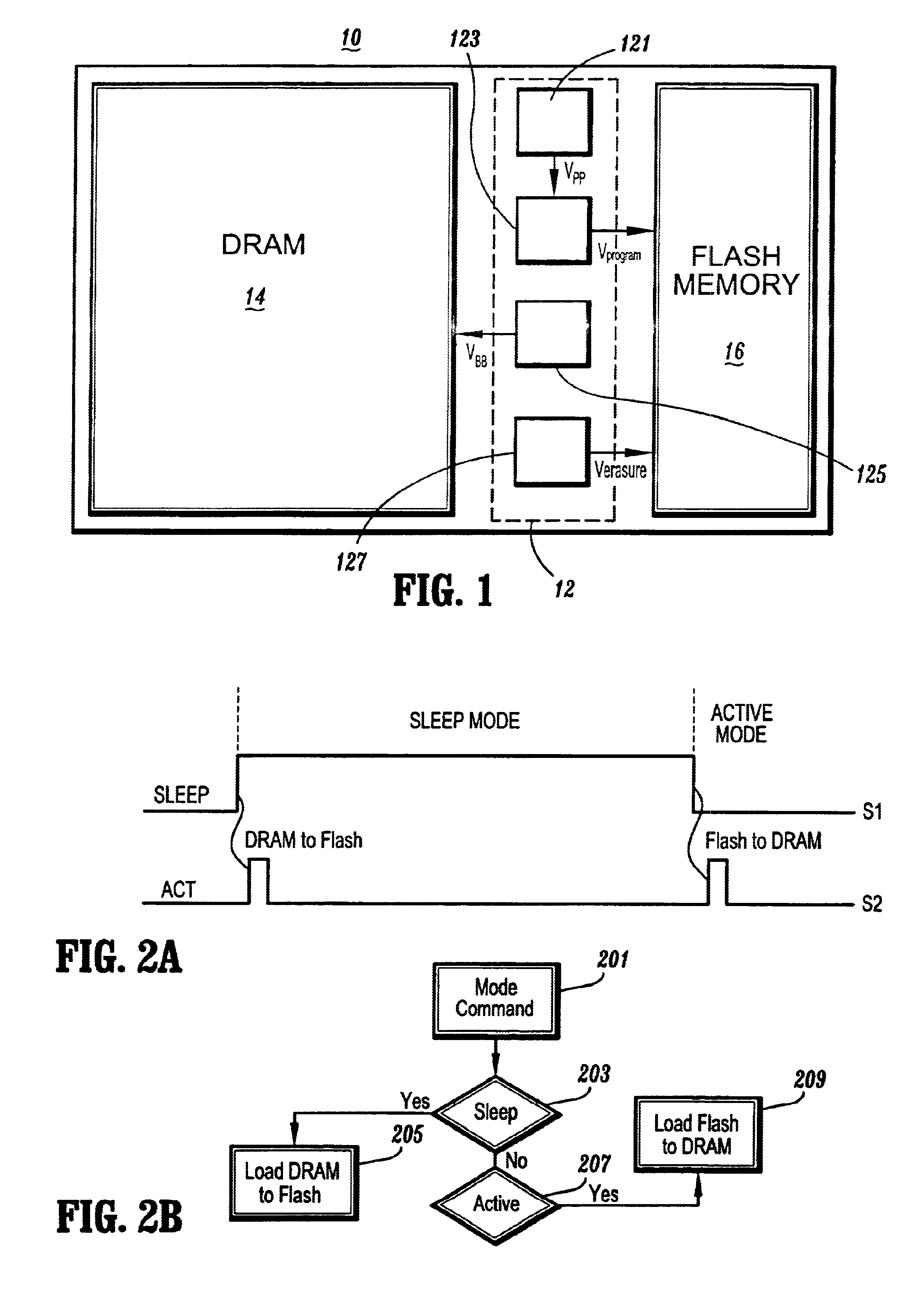
The present invention provides a method of fabricating a semiconductor memory device having volatile memory such as dynamic random access memory (DRAM) and non-volatile memory such as flash memory which are merged into a single chip using a system on-chip (SOC) design. Preferably, volatile and non-volatile memory devices are simultaneously built on a single chip by embedding volatile memory devices into non-volatile memory devices and vice versa. The fabrication process also includes integration on a single chip of support circuits for the memory devices. In the fabrication of the memory devices and support devices on a single chip, the present invention advantageously employs a simplified process in which steps for forming each device a...


PUM


Abstract

A method for fabricating DRAM and flash memory cells on a single chip includes providing a silicon substrate, forming a trench capacitor for each of the DRAM cells in the silicon substrate, forming isolation regions in the silicon substrate which are electrically isolated from each other, forming first type wells for DRAM and flash memory cells at first predetermined regions of the silicon substrate by implanting a first type impurity in the first predetermined regions, forming second type wells for DRAM and flash memory cells at second predetermined regions in the first type wells by implanting a second type impurity in the second predetermined regions, forming oxide layers for DRAM and flash memory cells on the second type wells, forming gate electrodes for DRAM and flash memory cells on the oxide layers for DRAM and flash memory cells, and forming source and drain regions for DRAM and flash memory cells in the respective second type wells for DRAM and flash memory cells, in which the source and drain regions are associated with each of the gate electrodes for DRAM and flash memory cells.

Description

1. Field of the InventionThe present invention relates to a method of fabricating semiconductor memory devices, and more particularly, to a method for integrating volatile and non-volatile memory devices on a single chip.2. Description of the Related ArtGenerally, electronic systems in various applications require, in addition to data processing units, memory devices to store data therein and / or read data therefrom. For enhanced performance, an electronic system may need dynamic random access memory (DRAM) devices and flash memory devices functionally or physically together. In this case, it is common that a DRAM device is used as temporary storage, and a flash memory device is used to store firmware and nonvolatile data. Such a combination of DRAM and flash memory devices can boost the system performance.Especially, in portable electronic products, such as laptops and palm computers, where battery lifetime is a limitation on the performance and functionality of electronic systems o...

Claims


Application Information

Patent Timeline
Patent Type & Authority Patents(United States)
IPC IPC(8): H01L21/70H01L21/8247H01L21/8242H01L27/105H01L21/8239
CPCH01L27/105H01L27/1052H01L27/11526H01L27/11546H01L27/10894H01L27/10861H10B99/00H10B12/038H10B12/09H10B41/40H10B41/49
Inventor HSU, LOUIS L.RADENS, CARL J.WANG, LI-KONG
Owner GOOGLE LLC
Why Eureka
Try Eureka