
Fingerprint image capture device with a passive sensor array

a fingerprint image and sensor array technology, applied in the field of fingerprint image capture devices with passive sensor arrays, can solve the problems of preventing the deployment of fingerprint sensors into security devices employed in consumer devices such as computers, wireless and hand-held devices, and other physical access control applications, which are all very cost sensitiv

Inactive Publication Date: 2004-01-06
LENOVO PC INT
View PDF10 Cites 131 Cited by
  • Summary
  • Abstract
  • Description
  • Claims
  • Application Information

AI Technical Summary

Problems solved by technology

One significant drawback of the above-mentioned silicon-based sensor arrays and the associated addressing and processing circuitry is the cost involved in integrating these on the same substrate.
As a result, the cost of each sensor chip can be significant.
This cost prevents deploying such fingerprint sensors into security devices employed in consumer devices such as computers, wireless and hand-held devices, internet appliances, and in other physical access control applications, which are all very cost sensitive.
In addition, most of the sensors that use CMOS type processing for the sensor array and associated electronics are adversely affected by ambient environmental conditions at the time of sensing and also by electrostatic discharge (ESD), if any.

Method used


Image

  • Fingerprint image capture device with a passive sensor array
  • Fingerprint image capture device with a passive sensor array
  • Fingerprint image capture device with a passive sensor array

Examples


Embodiment Construction

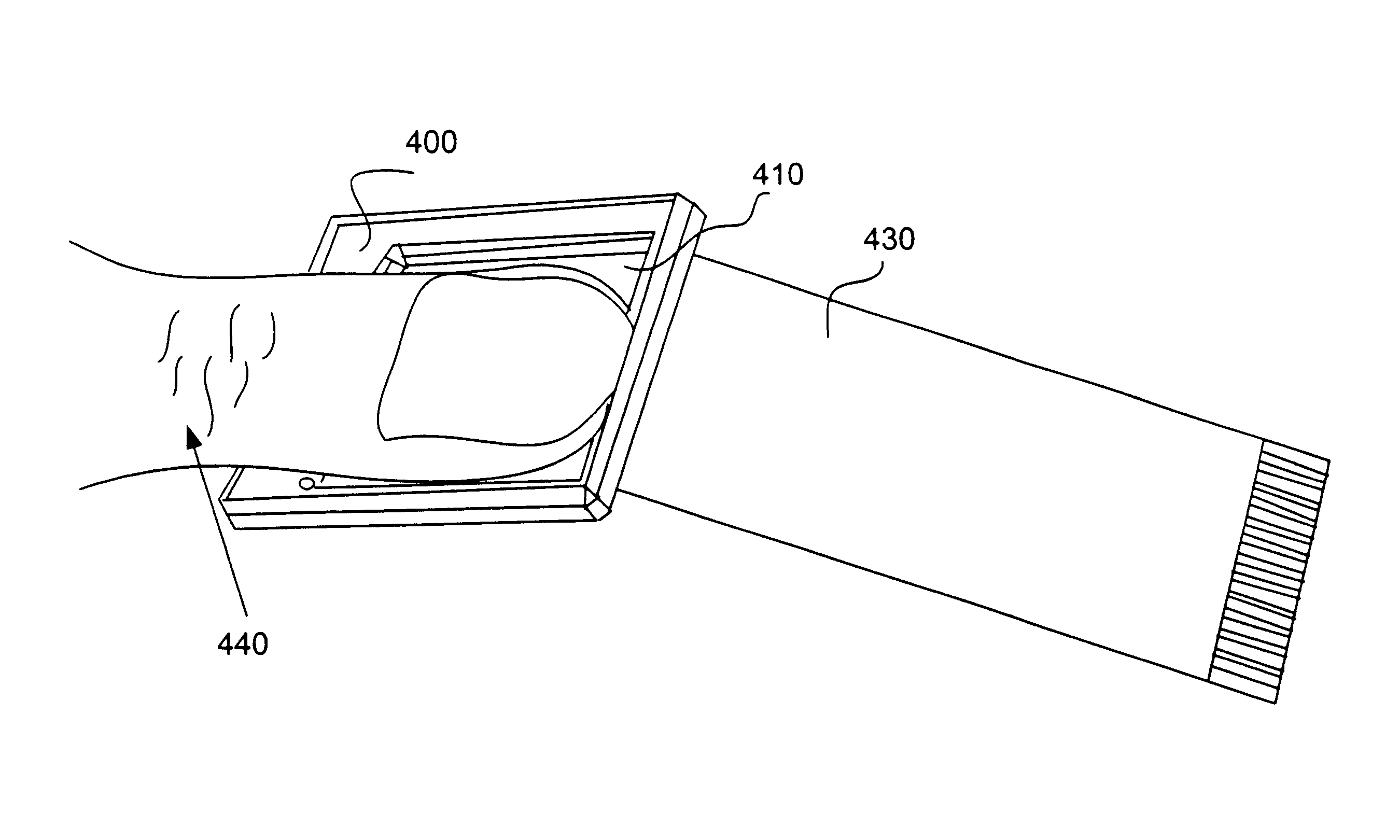
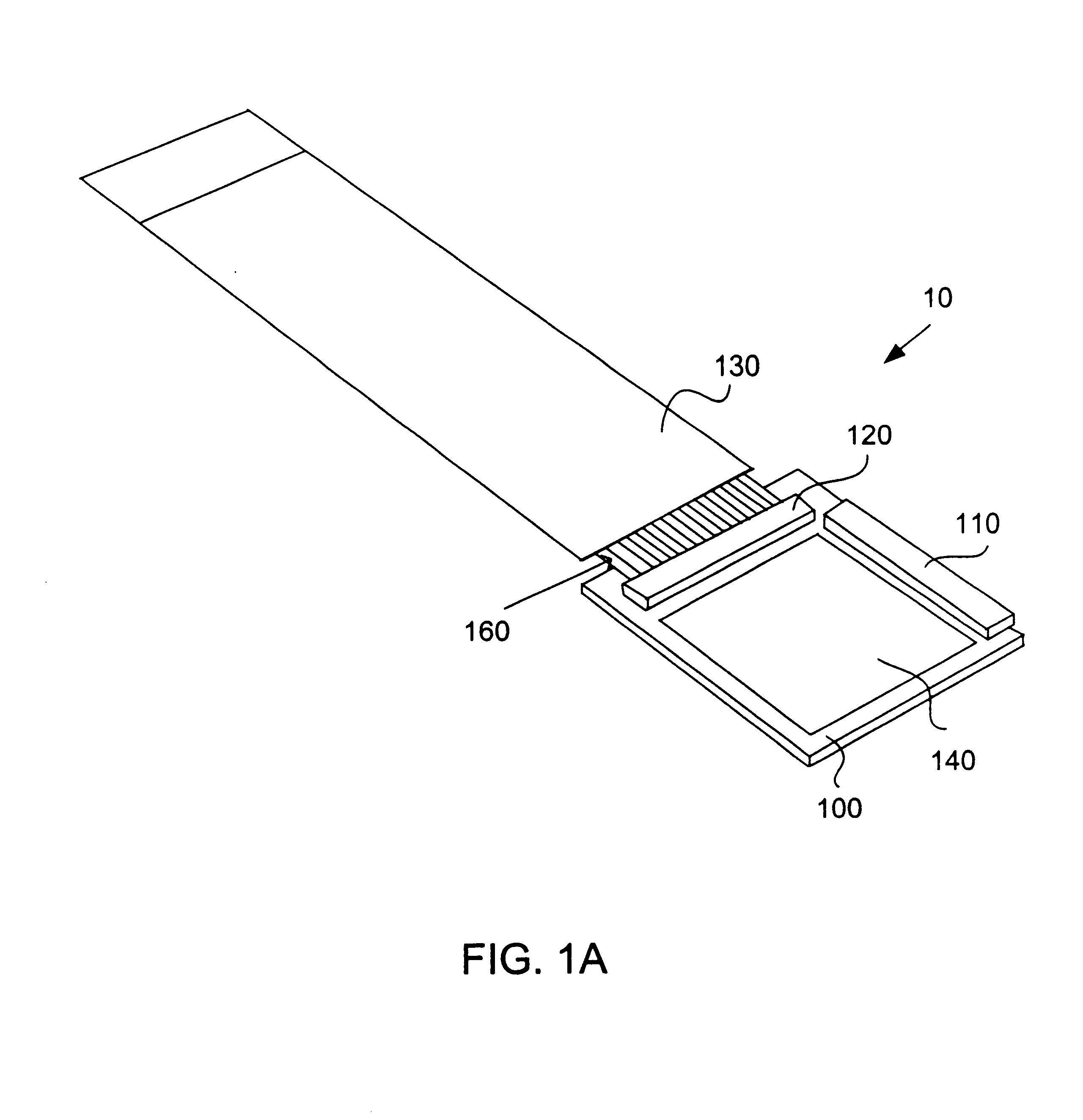
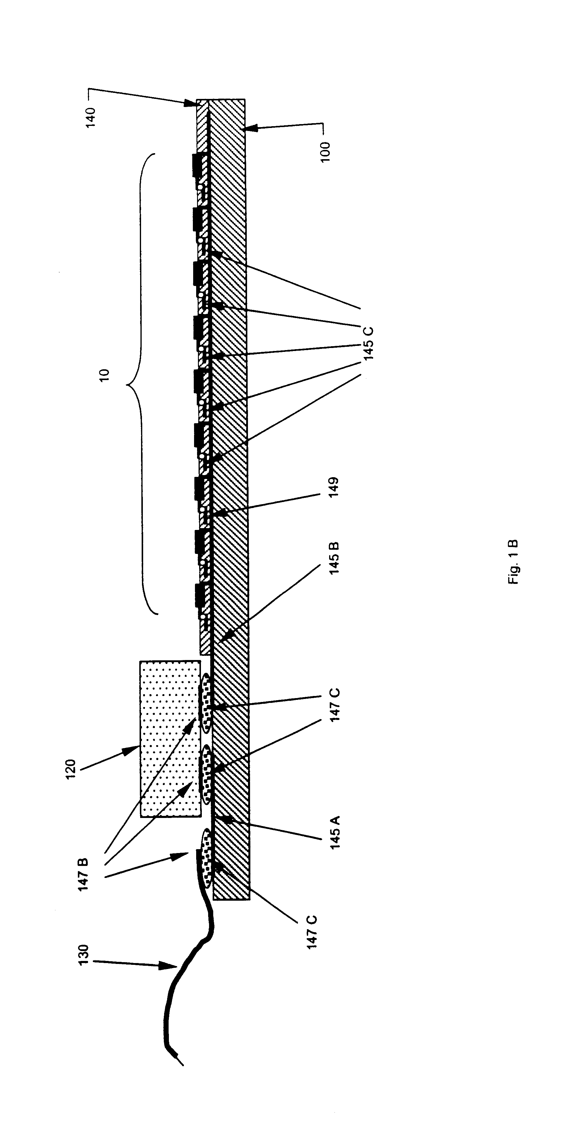
In brief, the invention consists of separating a fingerprint-sensor array that converts a fingerprint into resultant signals completely from sensor support integrated circuit(s) that contain addressing and processing circuitry used to address cells within the sensor array and process signals that are obtained which correspond to the textured surface placed upon the sensor array. The detected and processed signals can then be transmitted to other external devices without suffering from inordinate attenuation and thus become unusable in subsequent image processing that allows a fingerprint image to be rendered from the resultant signals. The sensing structure, which includes the sensor array and the base, with the corresponding interconnect structure therein, is fabricated independent of the sensor support integrated circuit(s) that contain the addressing and processing circuitry. The sensor array, in one embodiment, is composed of rows and columns of individual sensing cells, with on...


PUM

PropertyMeasurementUnit
diameteraaaaaaaaaa
resistanceaaaaaaaaaa
depthaaaaaaaaaa

Abstract

A fingerprint-sensing device with a sensor array that does not use active switching elements is fabricated on a base. Sensor support integrated circuits, which contain processing and addressing circuitry, are separately fabricated and subsequently mounted on the base, establishing electrical connections with an interconnect structure within the base, and are thus not integrated with the sensor array. The sensor support integrated circuits can be covered by a bezel structure and the sensor array by a covering material. In addition, a connection cable can be provided to connect the sensor array and the sensor support integrated circuits with a power source and to other external devices and to convey signals generated by the sensor array to the external devices.

Description

1. Field of the InventionThe invention relates generally to devices that sense textures and represent them using signals. More specifically, the invention relates to devices that sense fingerprints and other textured surfaces allowing them to thereby be represented as images.2. Related ArtThe fingerprint image sensing industry uses two prominent technologies to capture images of an individual's fingerprints for use in electronic security applications--(1) optical-based sensors, and (2) capacitance-based sensors. By design, most, if not all, such sensors employ a small-sized two-dimensional array of elementary sensor cells on a silicon chip. When a finger is placed on this small-sized sensor array, electronic circuitry scans each sensor cell in the sensor array for an applicable output. The output from each cell is a measure indicative of the distance between the fingerprint features (such as ridges) and the sensor cell at that location. A composite map of these distances translates ...

Claims


Application Information

Patent Timeline
Patent Type & Authority Patents(United States)
IPC IPC(8): G06K9/00
CPCG06K9/0002Y10T29/49002Y10T29/49007Y10T29/4913Y10T29/49128G06V40/1306
Inventor DECONDE, KEITH T.GANAPATHI, SRINIVASAN K.GLUCK, RANDOLPH S.HOVEY, STEVE H.PRAKASH, SHIVADOBKIN, ROBERT
Owner LENOVO PC INT
Learn More