Intralevel decoupling capacitor, method of manufacture and testing circuit of the same

a decoupling capacitor and manufacturing method technology, applied in the field of decoupling capacitors, can solve problems such as difficult yield problems, increase chip size, and create noise problems

Inactive Publication Date: 2004-01-13
GLOBALFOUNDRIES INC
View PDF30 Cites 67 Cited by
  • Summary
  • Abstract
  • Description
  • Claims
  • Application Information

AI Technical Summary

Problems solved by technology

Conventional microprocessor clock rates are approaching the gigahertz range of operation and thereby create noise problems.
However, large plate capacitors add significant critical area and thereby create a difficult yield problem.
On the other hand, trench capacitors require extra silicon area which increases the chip size.
Both solutions add significant process complexity and cost.

Method used


Image

  • Intralevel decoupling capacitor, method of manufacture and testing circuit of the same
  • Intralevel decoupling capacitor, method of manufacture and testing circuit of the same
  • Intralevel decoupling capacitor, method of manufacture and testing circuit of the same

Examples


Embodiment Construction

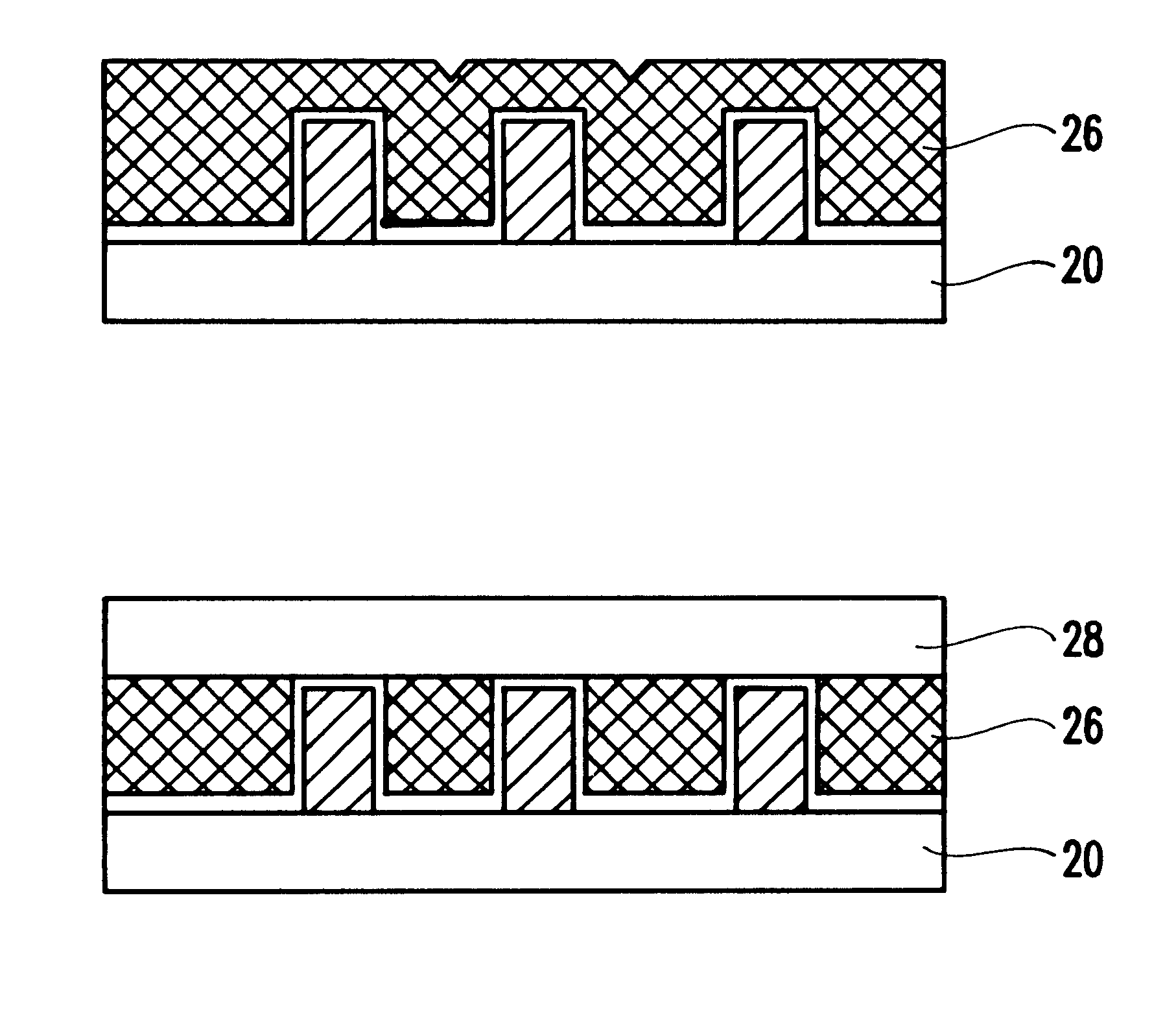
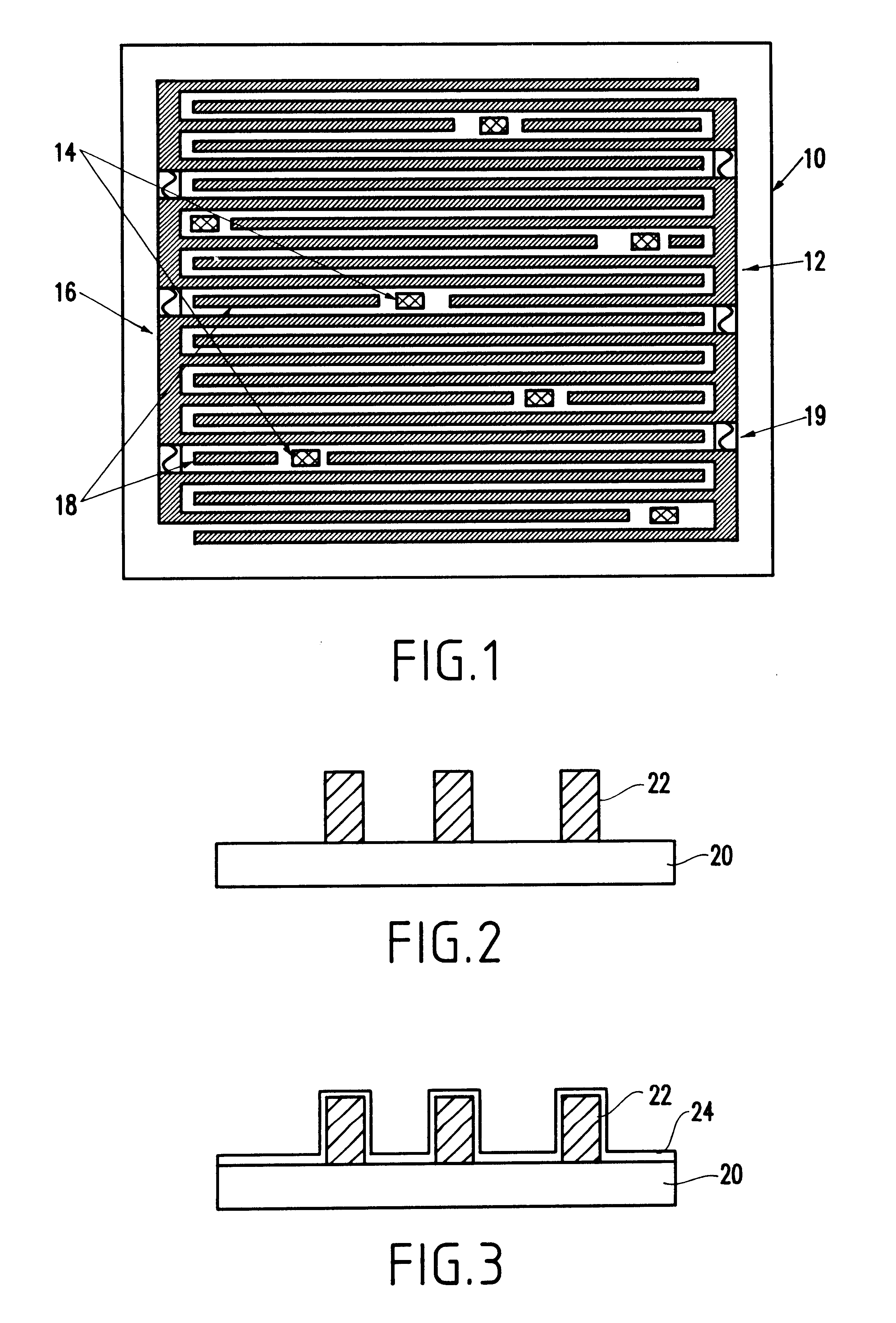
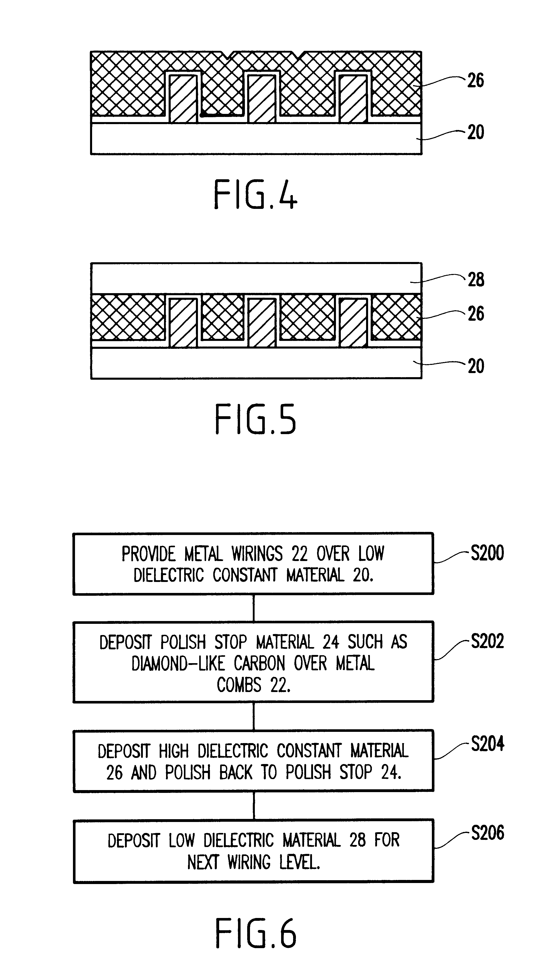
FIG. 1 illustrates a parallel plate capacitor structure. The finger capacitor may include interdigitized comb structures 12, 16 at a small (minimum) pitch constructed on a single wiring level. The comb structures 12, 16 occupy essentially the entire chip area 10 on a metal level above the active silicon surface. As is known in the art, ground comb 12 is connected to ground and power (V.sub.dd) comb 16 is connected to a power supply. Passthrough vias 14 may be provided for connections between upper and lower levels as is well known in the art. A pattern fill 18 may also be used following a break in the finger and the via 14 associated with that break.

This capacitor structure is preferably fabricated above the last wiring level so as to simplify the layout since the number of required passthrough vias 14 will be relatively small. The metal thickness and layout rules for this metal level may be the same as the minimum pitch wiring level. The capacitor structure may also utilize fuse li...


PUM

PropertyMeasurementUnit
dielectric constantaaaaaaaaaa
thickaaaaaaaaaa
thickaaaaaaaaaa

Abstract

A decoupling capacitor is provided for a semiconductor device and may include a first low dielectric insulator layer and a low resistance conductor formed into at least two interdigitized patterns on the surface of the first low dielectric insulator in a single interconnect plane. A high dielectric constant material may be provided between the two patterns. A circuit for testing a plurality of these capacitors is also provided which includes a charge monitoring circuit, a coupling circuit and a control circuit.

Description

1. Field of the InventionThe present invention generally relates to decoupling capacitors and more particularly to testing such capacitors having high dielectric material between the metal wirings of the capacitor.2. Description of the Related ArtConventional microprocessor clock rates are approaching the gigahertz range of operation and thereby create noise problems. As a result, large decoupling capacitors are used between a power supply and ground to provide enough noise immunity for proper circuit operation. Options include the integration of large plate capacitors, which would essentially occupy the entire chip above the active silicon surface, and trench capacitors embedded in the silicon substrate. However, large plate capacitors add significant critical area and thereby create a difficult yield problem. On the other hand, trench capacitors require extra silicon area which increases the chip size. Both solutions add significant process complexity and cost.In view of the foreg...

Claims


Application Information

Patent Timeline
Patent Type & Authority Patents(United States)
IPC IPC(8): H01L27/08H01L21/02
CPCH01G4/1272H01G4/35H01L23/5223H01L27/0805H01L22/22H01L28/60H01L23/642H01L28/40Y10T29/435H01L2924/3011H01L22/14H01L2924/0002H01L2924/00
Inventor BERNSTEIN, KERRYBRACCHITTA, JOHN A.COTE, WILLIAM J.NING, TAK H.PRICER, WILBUR D.
Owner GLOBALFOUNDRIES INC
Why Eureka
Try Eureka