Flat panel display device utilizing electron emission devices

a technology of electron emission and display device, which is applied in the manufacture of electric discharge tube/lamp, tubes with screens, discharge tubes luminescnet screens, etc., can solve the problems of high risk of bus electrode breakage, drawback of destruction of top electrode, and very thick insulator layer, and achieve stable electron emission without deterioration

Inactive Publication Date: 2004-03-02
PIONEER CORP
View PDF5 Cites 16 Cited by
  • Summary
  • Abstract
  • Description
  • Claims
  • Application Information

AI Technical Summary

Benefits of technology

The present invention has been conceived taking the above situation into consideration, and it is an object of the invention to provide a flat panel display device utilizing such electron emission sites capable of providing stable electron emission without deterioration.
As illustrated in FIG. 4, the top electrodes 15 formed on the insulator layer 13 are formed only in flat regions of the insulator layer at spaces associated with sub-pixels. The top electrodes 15 are formed on the flat surfaces of the insulator layer 13 with a uniform thickness without shaping the top electrodes themselves in the form of stripes. This makes it possible to generate a uniform electric field when they are driven. The connecting section (precipice portion) of each top electrode 15 is formed on the bus electrode 16 which is sufficiently thick. The top electrodes 15 of adjoining devices are connected by the bus electrode 16. While a bus electrode 16 is formed to cross a precipice portion that is formed because of the thickness of a bottom electrode, a semiconductor electron supply layer, and an insulator layer, since a sufficiently thick first insulating protective film 17a is provided under the bus electrode 16, any shorting between the electrode and the bottom electrode 11 or semiconductor electron supply layer 12 is prevented. The thickness of the bus electrodes 16 relative to the panel size may be any value as long as no problem associated with resistance occurs, a preferable thickness ranging from 0.1 to 50 .mu.m. The first insulating protective film 17a under the bus electrodes 16 may be provided before or after the insulator layer 13 at the pixel region is formed. The insulating protective films 17a make it possible to provide a device structure in which the bus electrodes 16 are not damaged because of the presence of the precipice.
In this panel, the bus electrodes 16 which are arranged in parallel in the direction orthogonal to the direction of the bottom electrodes 11 must be formed at a later step. The breakage of the bus electrodes 16 located on the top of the panel attributable to the difference between the thicknesses of the bottom electrodes 11 and electron supply layers 12 is prevented by providing the first insulating protective films 17a.
Next, as shown in FIG. 4, the top electrodes 15 are formed as individual electrodes in the form of islands to be linked by the bus electrodes 16. Each of the top electrodes 15 is formed across the bus electrodes 16, second insulating protective films 17b, and insulator layer 13 such that a major part of the same is located on a flat surface of the insulator layer 13 and such that an edge of the same covers a part of a bus electrode 16. The first insulating protective films 17a isolate the bus electrodes 16 and isolate adjoining devices from each other, and the second insulating protective films 17b isolate the bus electrodes 16 from the insulator layer 13. Since the distance from the electron supply layer 12 to the top electrode 15 in a region where the second insulating protective film 17b is formed is greater than a similar distance in a region where no second insulating protective film 17b is formed, it is possible to prevent a leak current from the bottom of the bus electrodes 16 and the bottom of the top electrodes 15 on the way to the emitting section.
The thickness of the first insulating protective films 17a in the above-described embodiment may be set at a value that is similar to or greater than the thickness up to the electron supply layer 12 as shown in FIG. 7, this is not limiting the present invention. For example, breakage of the bus electrodes can be avoided if the films have a thickness that is 5% or more of the thickness of the electron emission sites as shown in FIG. 11. Therefore, the thickness of the first insulating protective films is preferably 5% or more of the thickness of the devices as a whole (about 6 .mu.m) (the upper liming being a thickness that is substantially equal to the height of the device insulator layer 13). The lower limit for the thickness of the first insulating protective films 17a is a thickness which does not cause breakage of the bus electrodes. Further, as shown in FIG. 12, even if there is no first insulating protective film, each of second insulating protective films 17b having a thickness ranging from 5% or more of the total thickness of the device to 5 .mu.m avoids the breaking of the bus electrode as well as the top electrode as an advantageous effect of the invention. The second insulating protective films 17b facilitates to improve the freedom of design for the display panel without line breakage.

Problems solved by technology

As a result, a high resistivity of the thin portion of the top electrode causes an uneven electric field to bring a drawback of destruction in the top electrode.
However, the uneven electric field caused by the thin portion's high resistivity in the top electrode still appears with a risk of breakage of the bus electrode in the case that the thickness of the stacked layers, particularly, the insulator layer is very thick, since no insulating protective film is formed on the backside substrate between the adjacent electron emitting sections.
In such a condition, alkaline components leak from the backside substrate of glass to react with the top electrode directly contacted and then migration and electrode corrosion occur in the top electrode.
As a result, there is a problem that reduction of the electric field to be normally supplied to the electron emitting section of the upper thin-film metal electrode.

Method used


Image

  • Flat panel display device utilizing electron emission devices
  • Flat panel display device utilizing electron emission devices
  • Flat panel display device utilizing electron emission devices

Examples


Embodiment Construction

flat panel display device was actually fabricated with specifications (1) through (6) as shown below, and then characteristics of the same were examined.

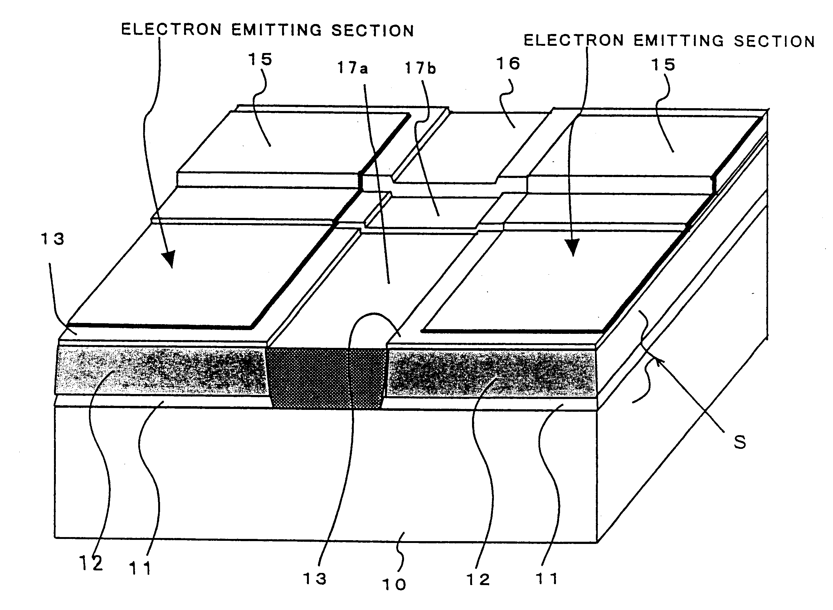
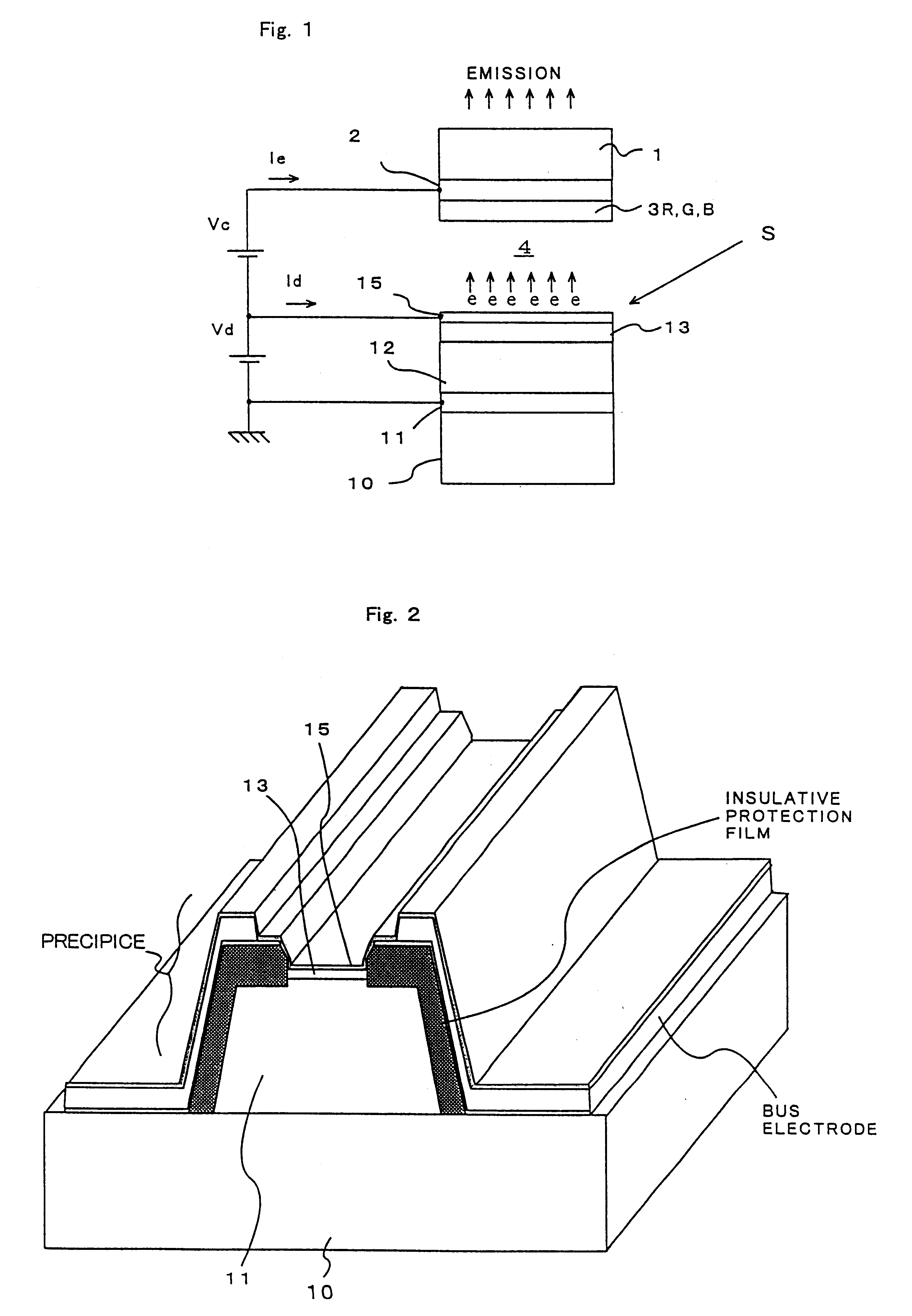
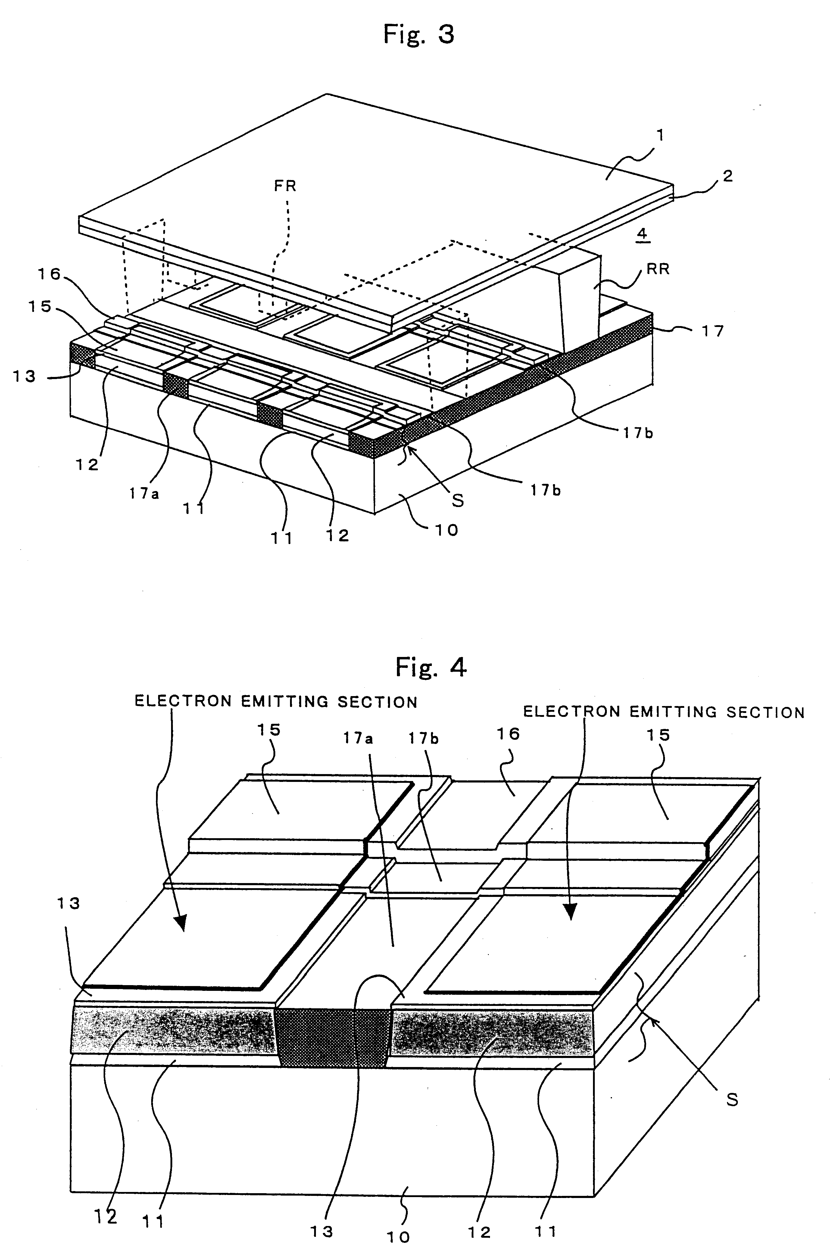
(1) Bottom electrodes: Cr, Cu, and Cr films having thicknesses of 50 nm, 1 .mu.m, and 100 nm, respectively.

(2) Semiconductor electron supply layer: Si layer having a thickness of 4 .mu.m.

(3) Insulator layer: SiO.sub.x layer having a thickness of 330 nm.

(4) Top electrode: Pt film having a thickness of 40 nm.

(5) Bus electrodes: Cr, Cu, and Cr films having thicknesses of 50 nm, 1 .mu.m, and 100 nm, respectively.

(6) Insulating protective films to be under the bus electrode: SiO.sub.x films having a thickness of 350 nm.

The bottom electrodes (1) and semiconductor electron supply layers (2) were formed in the form of lines on a glass substrate which had been cleaned. Thereafter, the first insulating protective films to be under the bus electrode (6) were formed between the lines. Next, the insulator layers (3) were formed on the semiconduc...


PUM


Abstract

A display device includes a backside and a front-side substrates facing each other with a vacuum space therebetween; and a plurality of electron emission sites provided on the backside substrate. Each electron emission sites includes a bottom electrode formed on a surface of the backside substrate proximate to the vacuum space, an insulator layer formed over the bottom electrode, and a top electrode formed on the insulator layer and arranged individually apart from each other and facing the vacuum space. The display device also includes a plurality of bus electrodes for electrically connecting the neighboring top electrodes; and insulating protective films each provided between the bus electrode and the insulator layer and between the bus electrode and the backside substrate.

Description

1. Field of the InventionThe present invention relates to an electron emission device and a display apparatus using the same, especially to a flat panel display apparatus in which a plurality of the electron emission devices are arranged in an image display array, i.e. in a matrix arrangement.2. Description of the Related ArtConventionally, FEDs (field emission display devices) are known as flat type light-emitting display devices having an array of cool-cathode type electron emission sources whose cathodes are not required to be heated. It is necessary to unitize the flat type display device utilizing FEDs to develop an ultra-large display unit system for a next generation. Electron emitting devices as electron emission sources of FEDs include devices having a metal-insulator-semiconductor (MIS) structure and devices having a metal-insulator-metal (MIM) structure.As shown in FIG. 1, an electron emission device having the MIS structure has a diode structure in which a top electrode ...

Claims


Application Information

Patent Timeline
Patent Type & Authority Patents(United States)
IPC IPC(8): H01J31/12H01J29/04H01J1/312
CPCB82Y10/00H01J1/312H01J31/127H01J2201/3125
Inventor CHUMAN, TAKASHIYOSHIKAWA, TAKAMASAHATA, TAKUYASAKEMURA, KAZUTOYAMADA, TAKASHINEGISHI, NOBUYASUIWASAKI, SHINGOSATOH, HIDEOYOSHIZAWA, ATSUSHIOGASAWARA, KIYOHIDE
Owner PIONEER CORP
Why Eureka
Try Eureka