
Deposited film forming apparatus

a film forming and film technology, applied in the field of deposited film forming apparatus, can solve the problems of difficult to induce the glow discharge itself, degrade the transmission characteristics of high-frequency power, and abnormal growth

Inactive Publication Date: 2004-03-09
CANON KK
View PDF12 Cites 41 Cited by
  • Summary
  • Abstract
  • Description
  • Claims
  • Application Information

AI Technical Summary

Problems solved by technology

The principal cause of the image defects is in that the deposited film peels off and scatters onto the substrate resulting in abnormal growth.
It was also found that with the frequencies over 450 MHz the transmission characteristics of the high-frequency power were degraded and there were some cases in which it was difficult to induce the glow discharge itself.

Method used


Image

  • Deposited film forming apparatus
  • Deposited film forming apparatus
  • Deposited film forming apparatus

Examples


experiment 1

(Experiment 1)

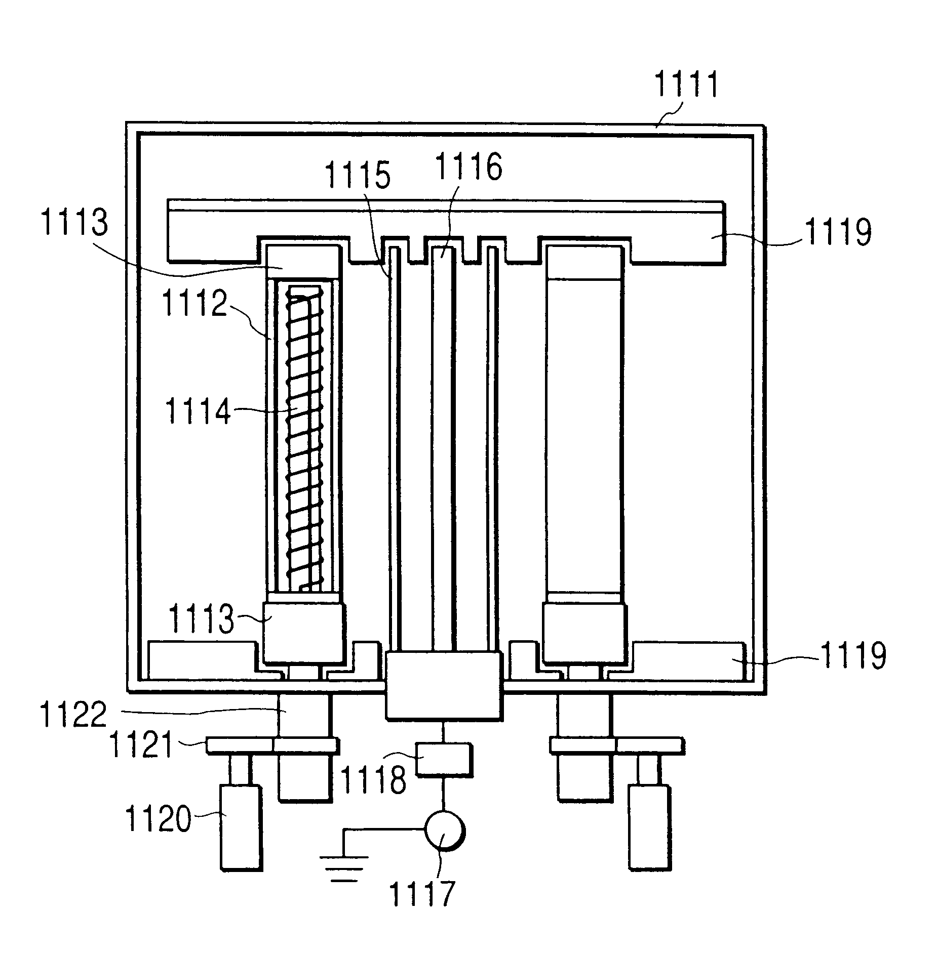
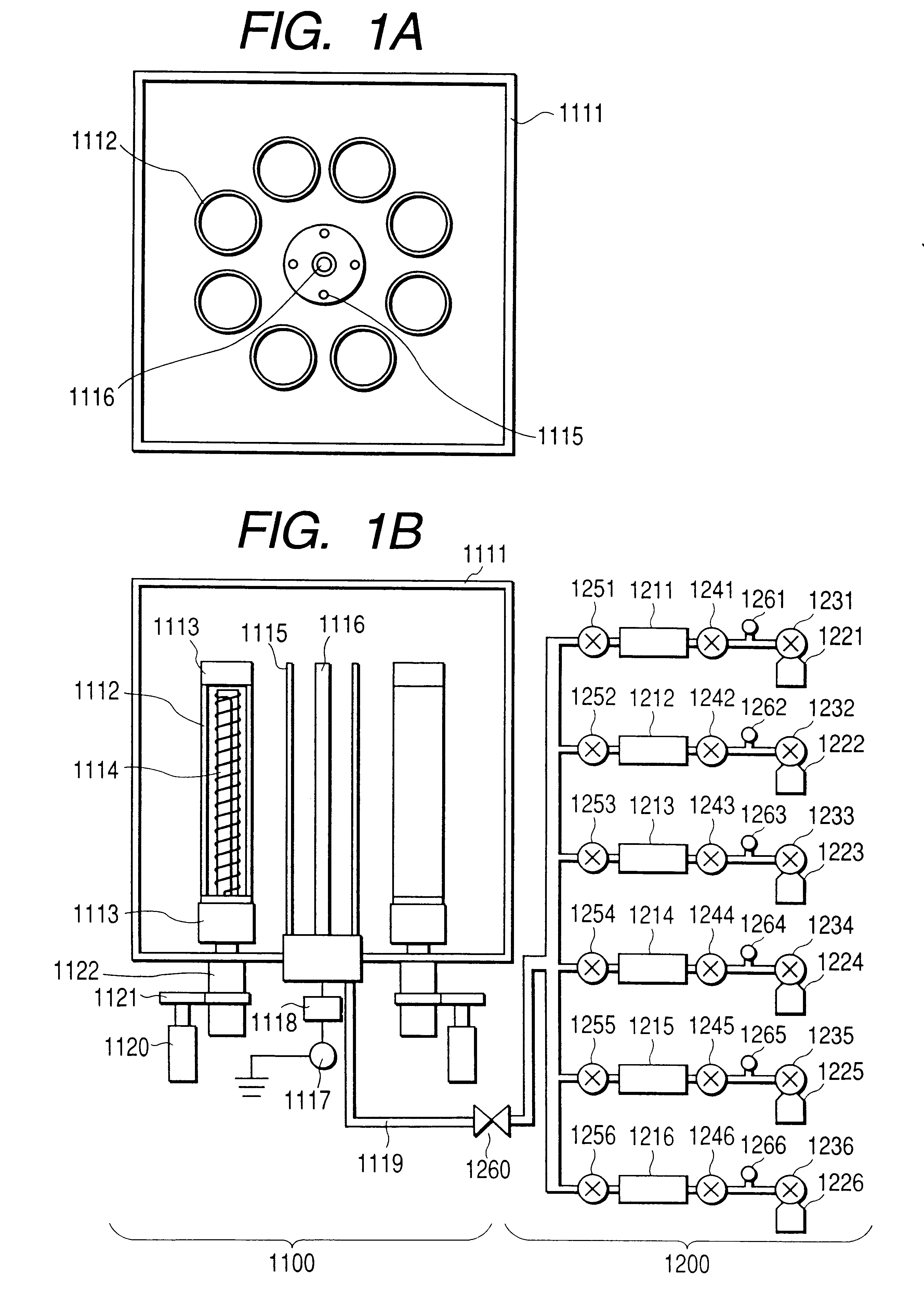
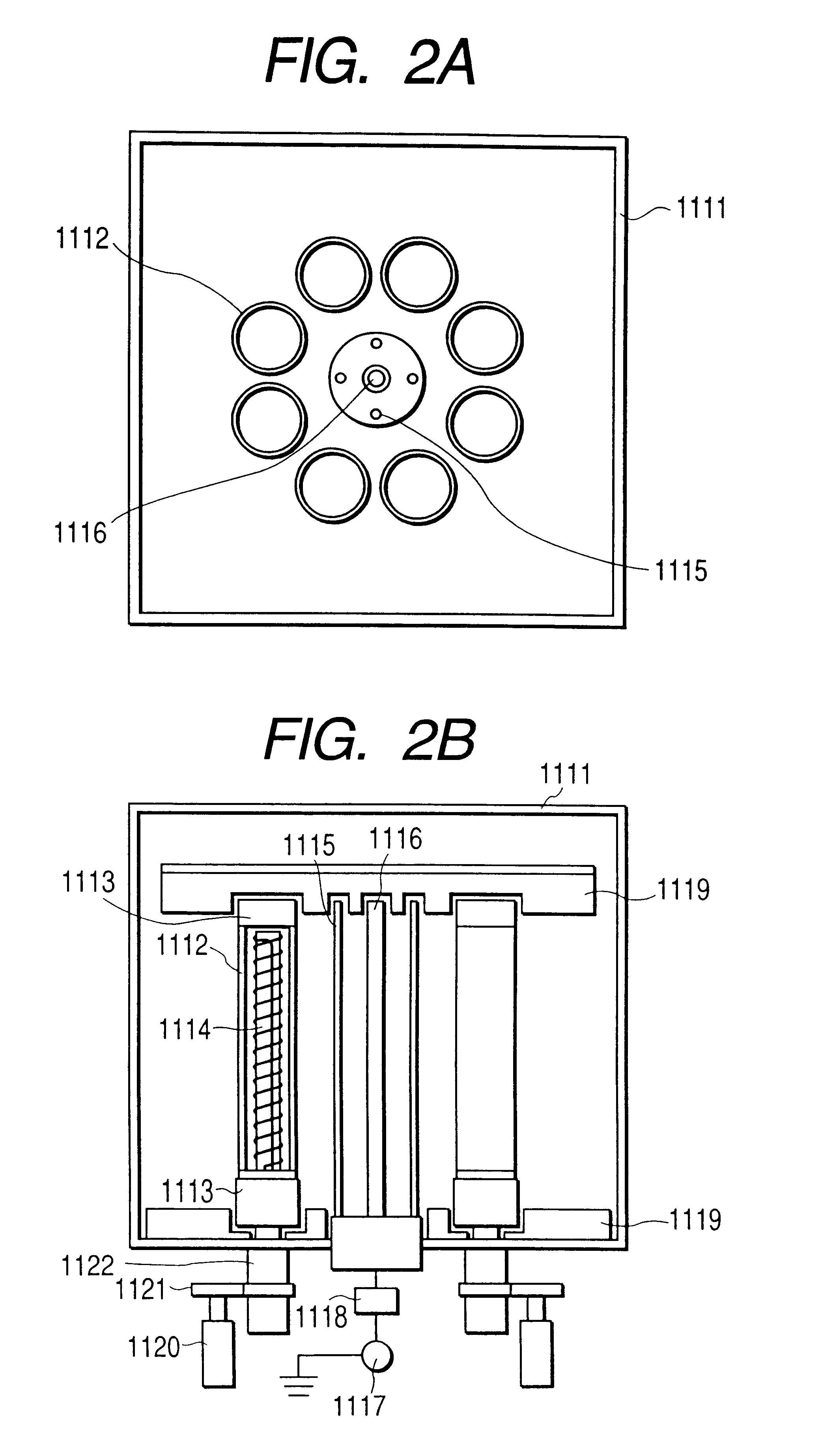
In the deposited film forming apparatus of the present invention illustrated in FIGS. 2A and 2B where the end portions of all the gas inlet pipes, the cathode electrode, and the holding members of the cylindrical substrates were located outside the glow discharge inducing area, the stability of discharge was evaluated according to the method described below under the conditions shown in Table 1 below, on surface-mirror-finished, aluminum cylinders (cylindrical substrates) of the outside diameter of 80 mm and the length of 358 mm. The means for locating all the end portions of the gas inlet pipes, cathode electrode, and holding members of cylindrical substrates was end covering members 4119 comprised of Al.sub.2 O.sub.3 and machined so that the depth of each groove was 2 cm and a clearance with respect to each end portion of the gas inlet pipes, cathode electrode, and holding members of cylindrical substrates was 2 mm, as illustrated in FIGS. 6A and 6B. The surface roug...

example 1

In the deposited film forming apparatus illustrated in FIGS. 2A and 2B, the end covering members 4119, similar to those in Experiment Example 1 illustrated in FIGS. 6A and 6B, were set as the means for locating all the end portions of the gas inlet pipes, cathode electrode, and holding members of cylindrical substrates outside the glow discharge inducing area, and electrophotographic photosensitive members each comprised of the charge injection inhibiting layer, the photoconductive layer, and the surface layer were produced at the oscillation frequency of the high-frequency power supply of 105 MHz under the production conditions shown in Table 4, on each of surface-mirror-finished, aluminum cylinders (cylindrical substrates) having the outside diameter of 80 mm and the length of 358 mm.

example 2

In the deposited film forming apparatus illustrated in FIGS. 2A and 2B, the end covering members 4119, similar to those in Experiment 1 illustrated in FIGS. 6A and 6B, were set as the means for locating all the end portions of the gas inlet pipes, cathode electrode, and holding members of cylindrical substrates outside the glow discharge inducing area, and the electrophotographic photosensitive members each comprised of the charge injection inhibiting layer, the photoconductive layer, and the surface layer were produced under the production conditions of Table 4 on each of surface-mirror-finished, aluminum cylinders (cylindrical substrates) having the outside diameter of 80 mm and the length of 358 mm. Evaluations similar to those in Example 1 were carried out. However, film formation was carried out at each of different oscillation frequencies of the high-frequency power supply ranging from 13.56 MHz to 500 MHz. The results obtained are shown in Table 6.

As seen from Table 6, the go...


PUM

PropertyMeasurementUnit
temperatureaaaaaaaaaa
frequencyaaaaaaaaaa
surface roughnessaaaaaaaaaa

Abstract

For enhancing plasma uniformity and long-term stability so as to readily form a film with excellent uniformity of thickness and quality and with good repeatability and for suppressing occurrence of image defects and drastically increasing the yield to form a deposited film ready for volume production, particularly, a functional deposit film (for example, an amorphous semiconductor used for semiconductor devices, electrophotographic photosensitive members, photovoltaic devices, and so on) is formed in an apparatus including a reaction vessel which can be hermetically evacuated, a substrate holder in the reaction vessel, a source gas supply, a power supply for high-frequency power. An end covering member is provided at an end of each of the substrate holder, the source gas supply and the power supply.

Description

1. Field of the InventionThe present invention relates to a deposited film forming apparatus (a plasma CVD apparatus etc.) and a deposited film forming method for forming a deposited film, particularly a functional deposited film (for example, an amorphous semiconductor used for semiconductor devices, electrophotographic photosensitive members, photovoltaic devices, and so on) or the like, on a substrate.2. Related Background ArtSuggested as device materials used for the semiconductor devices, electrophotographic photosensitive members, photovoltaic devices, and various other electronic devices are non-monocrystalline deposited films such as amorphous silicon, for example, typified by amorphous silicon compensated by hydrogen or / and halogen (for example, fluorine, chlorine, etc.) (which will hereinafter be abbreviated as "a-Si:H,X"), or crystalline deposited films such as thin films of diamond, and some of them are used in practice. These deposited films are formed, for example, by ...

Claims


Application Information

Patent Timeline
Patent Type & Authority Patents(United States)
IPC IPC(8): C23C16/509C23C16/50H01J37/32G03G5/08H01L21/205
CPCC23C16/509H01J37/32623
Inventor HOSOI, KAZUTOSHIRASUNA, TOSHIYASUTAKADA, KAZUHIKOOKAMURA, RYUJIAKIYAMA, KAZUYOSHIMURAYAMA, HITOSHI
Owner CANON KK
Learn More