Method and apparatus for direct connection between two integrated circuits via a connector

a technology of integrated circuits and connectors, applied in the field of high-speed direct connection between integrated circuits, can solve the problems of high cost of mcm technology, particularly acute noise and impedance effects, and undesirable effects of mcm technology

Inactive Publication Date: 2004-03-16
GLOBALFOUNDRIES US INC
View PDF40 Cites 93 Cited by
  • Summary
  • Abstract
  • Description
  • Claims
  • Application Information

AI Technical Summary

Problems solved by technology

The noise and impedance effects that result from routing a bus through the printed circuit board are to particularly acute for high speed buses, especially where relatively long traces (e.g., over three inches) have to be used for the communication path.
However, such MCM technology is costly and therefore undesirable for applications such as desktop personal computers.

Method used


Image

  • Method and apparatus for direct connection between two integrated circuits via a connector
  • Method and apparatus for direct connection between two integrated circuits via a connector
  • Method and apparatus for direct connection between two integrated circuits via a connector

Examples


Embodiment Construction

)

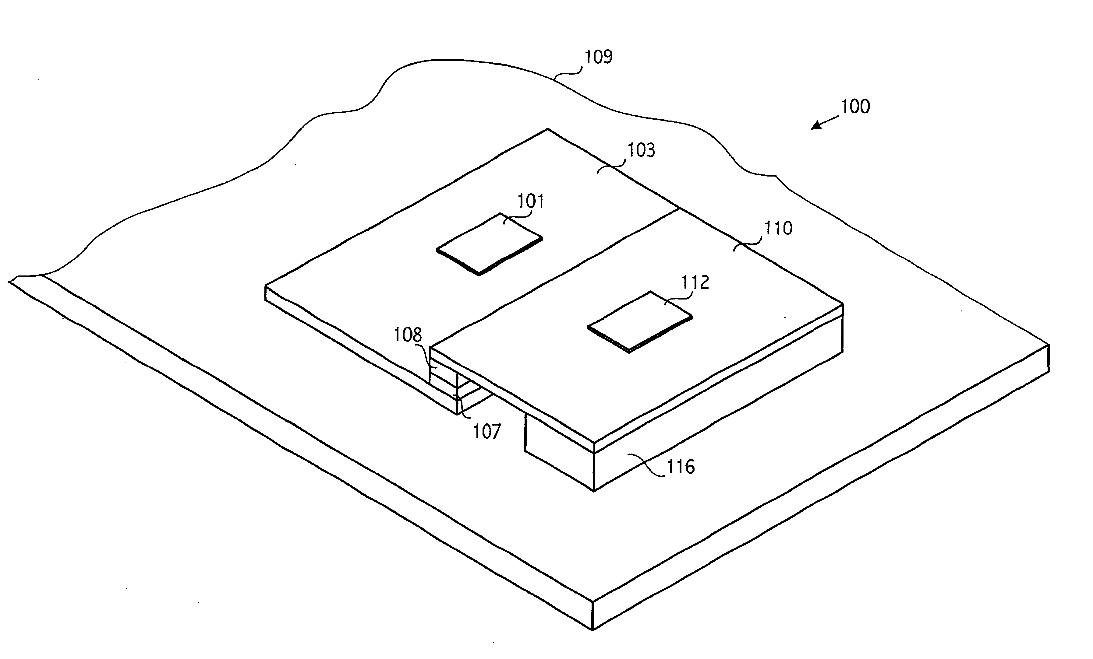
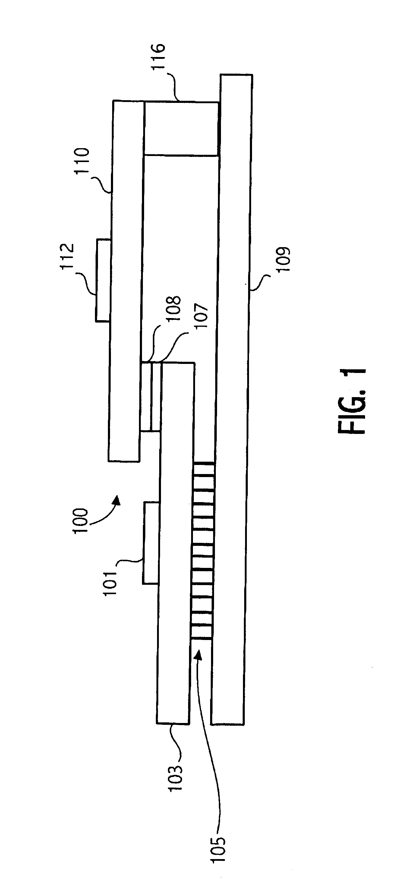
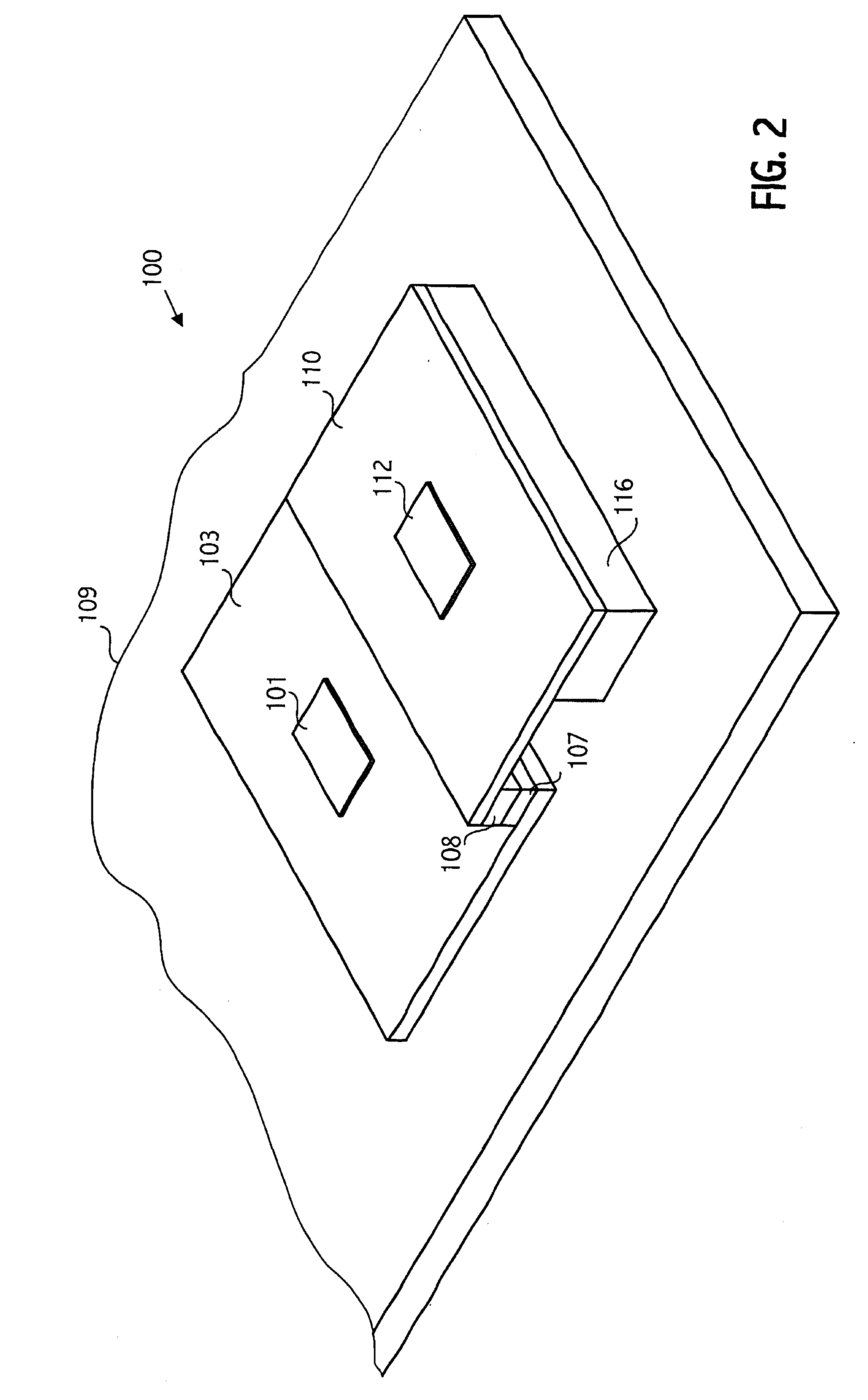
Referring to FIG. 1, an exemplary embodiment shows an integrated circuit assembly that includes integrated circuit die 101 mounted on package 103. Package 103 includes two sets of electrical connections. One set of electrical connections is shown as contacts 105 on the bottom surface of package 103. In the illustrated embodiment, contacts 105 electrically connect with printed circuit board 109. In another embodiment, the contacts 105 may connect to printed circuit board 109 through an intermediate device such as a socket. A high density / high speed electrical connector 107 provides a second set of electrical connections on the top surface of package 103.

Also shown in FIG. 1 is package 110 on which is mounted integrated circuit die 112. Package 110 also includes two sets of electrical connections, a mating high speed connector 108 that couples to connector 107 and a set of electrical contacts (not shown in FIG. 1) that connect to circuit board 109 through an intermediate connection (...


PUM


Abstract

A first package for an integrated circuit has both a first set of electrical contacts and a first connector. A second package has a second set of electrical contacts and a second connector. The first and the second connector are mating connectors that are electrically and physically coupled. The first set of electrical contacts and the first connector are disposed on opposite surfaces of the first package and the second set of electrical contacts and the second connector are disposed on the same surface of the second package. The first and second set of electrical contacts couple to a printed circuit board directly or indirectly through a socket. The connectors allow higher speed signals to be routed over the first and second connectors, while power, ground and slower speed signals can be routed over the first set and second set of electrical contacts.

Description

1. Field of the InventionThis invention relates generally to integrated circuits and more particularly to high speed direct connection between integrated circuits.2. Description of the Related ArtIn electronic devices such as personal computers, an integrated circuit such as the microprocessor, typically communicates with other integrated circuits via buses, which are formed physically as traces in a printed circuit board (PCB). Most integrated circuits (ICs) are packaged in plastic or ceramic packages or are otherwise encapsulated to protect the device. Pins or other contacts connect the package to the printed circuit board. There are a wide variety of packages and packaging techniques used for integrated circuits including dual inline packages (DIP), pin grid array (PGA) packages, land grid array (LGA) packages, and ball grid array (BGA) packages. DIPs provide two rows of connectors on the periphery of the package. PGA packages provide an array of pins on the bottom surface of the...

Claims


Application Information

Patent Timeline
Patent Type & Authority Patents(United States)
IPC IPC(8): H05K7/10H05K1/18H05K1/02
CPCH05K1/181H05K7/1092H05K1/0237H05K2201/10303H05K2201/10325H05K2201/1053H05K2201/1059H05K2201/10689H05K2201/10734Y02P70/50
Inventor ANDRIC, ANTHONY M.HILL, RUELMARKWARDT, DOUG
Owner GLOBALFOUNDRIES US INC
Why Eureka
Try Eureka