Method and apparatus for wafer-to-wafer control with partial measurement data

Inactive Publication Date: 2004-03-16
ADVANCED MICRO DEVICES INC
View PDF1 Cites 70 Cited by
  • Summary
  • Abstract
  • Description
  • Claims
  • Application Information

AI Technical Summary

Problems solved by technology

Subsequent processes performed on the wafers may lack the benefit of efficient metrology data analysis of the same wafers.
If a second process performed on the semiconductor wafers 105 were performed immediately after the first process, it would be difficult to deliver correction data for implementation into the subsequent process.
The process flow described in FIG. 2 provides for performing feed-forward corrections, although not necessarily in an efficient manner.
Interruptions in the process flow can also cause delay in delivery of products made from semiconductor wafers and other costs.
The interruption suffered by the manufacturing line to produce feed-forward data can cause ineffic

Method used


Image

  • Method and apparatus for wafer-to-wafer control with partial measurement data
  • Method and apparatus for wafer-to-wafer control with partial measurement data
  • Method and apparatus for wafer-to-wafer control with partial measurement data

Examples


Embodiment Construction

Illustrative embodiments of the invention are described below. In the interest of clarity, not all features of an actual implementation are described in this specification. It will of course be appreciated that in the development of any such actual embodiment, numerous implementation-specific decisions must be made to achieve the developers' specific goals, such as compliance with system-related and business-related constraints, which will vary from one implementation to another. Moreover, it will be appreciated that such a development effort might be complex and time-consuming, but would nevertheless be a routine undertaking for those of ordinary skill in the art having the benefit of this disclosure.

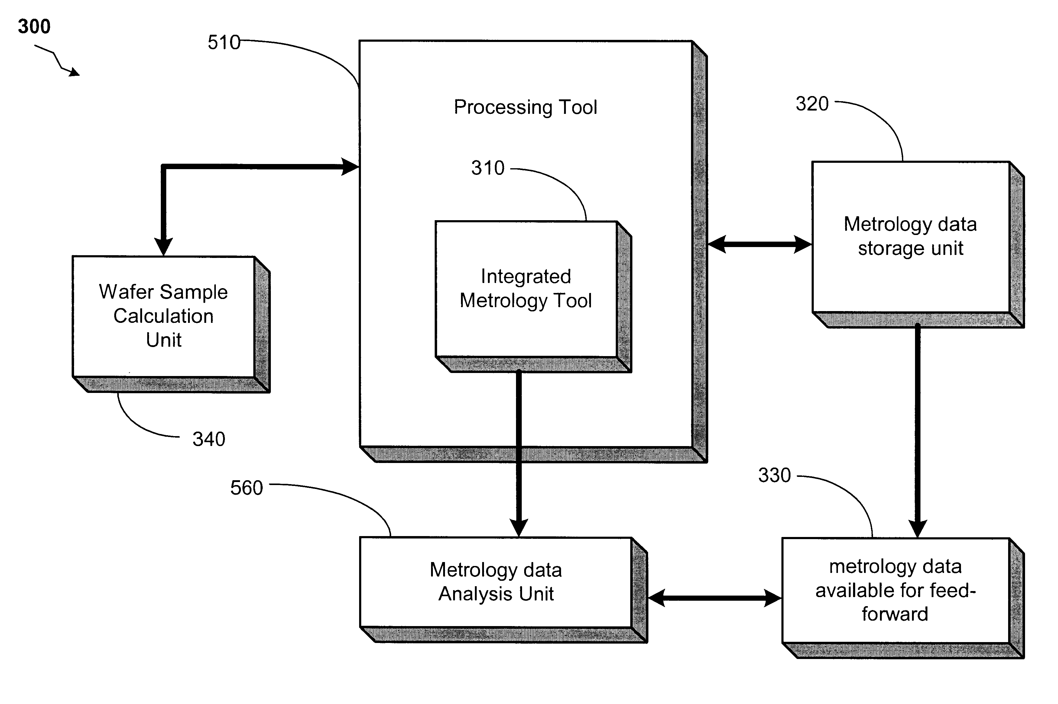
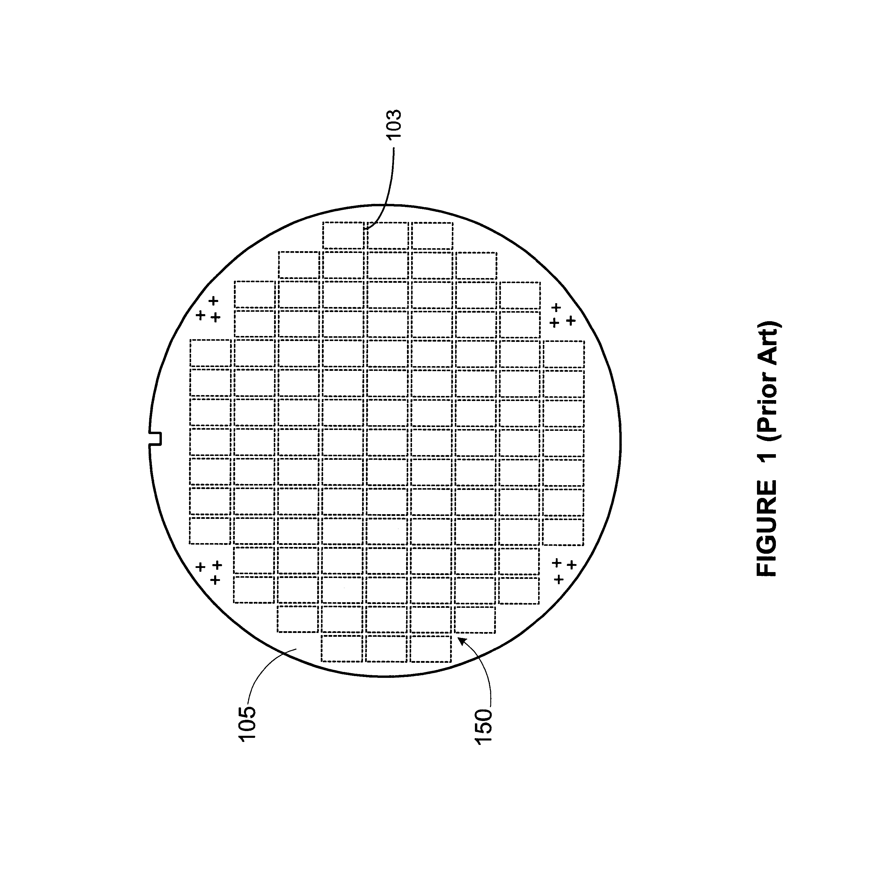
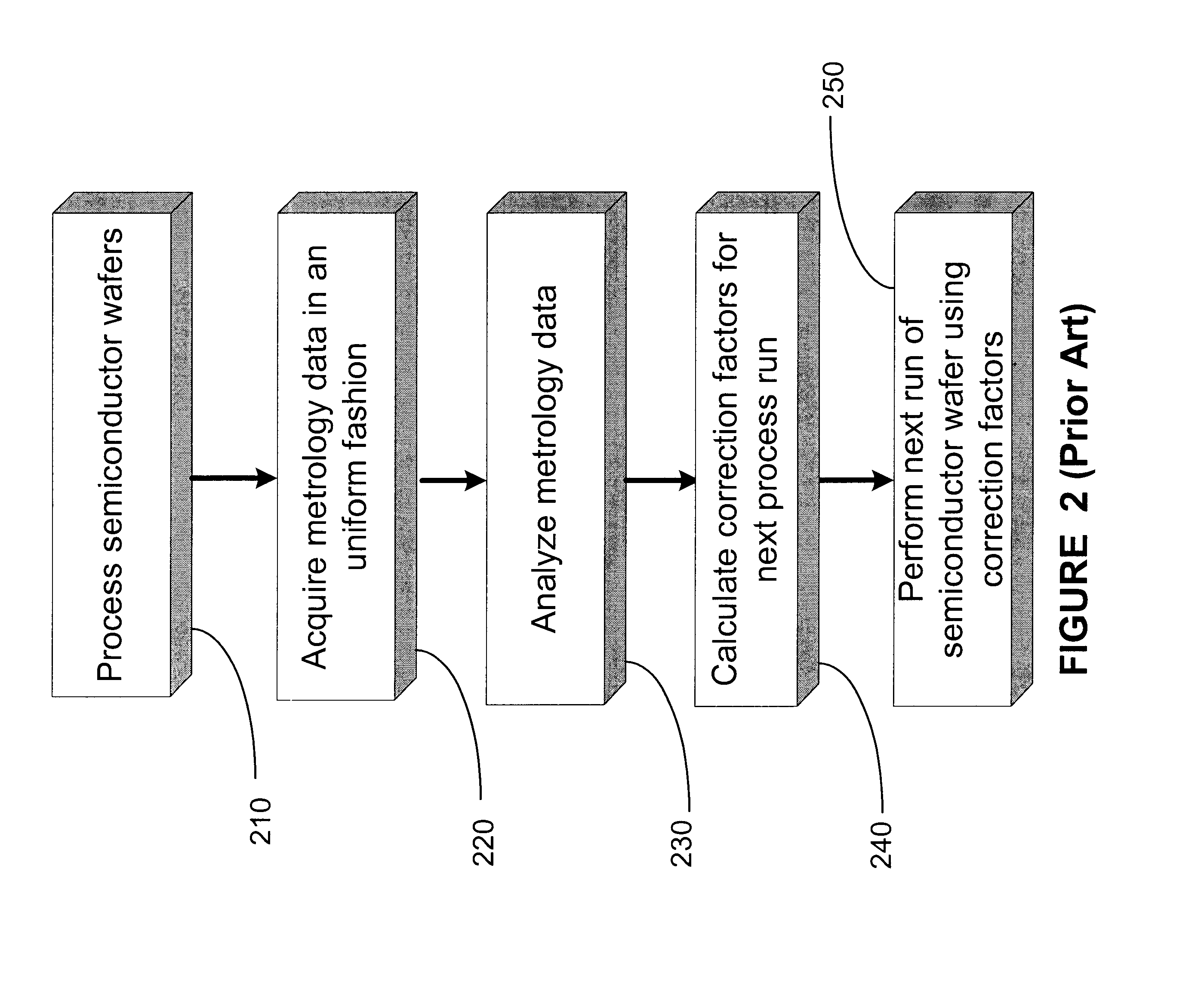
There are many discrete processes that are involved in semiconductor manufacturing. Many times, semiconductor devices are stepped through multiple manufacturing process tools. Often, at least a portion of a manufacturing lot of semiconductor wafers are examined by offline metrology too...


PUM


Abstract

A method and an apparatus for performing a process control using partial measurement data. A process operation is performed on a semiconductor wafer. Inline metrology data related to the process of the semiconductor wafer is acquired. A partial measurement data acquisition process is performed based upon the inline metrology data, the partial measurement data acquisition process comprising determining a time period for acquiring the inline metrology data, determining a number of wafers to be sampled based upon the time period, and determining a number of wafer sites for data acquisition. At least one of a feedback adjustment on a second semiconductor wafer and a feed-forward adjustment relating to a subsequent processing of the first semiconductor wafer based upon the partial measurement data acquisition process is performed.

Description

1. Field of the InventionThis invention relates generally to semiconductor manufacturing, and, more particularly, to a method and apparatus using metrology data from an integrated source for performing sampling of semiconductor wafer in a process flow.2. Description of the Related ArtThe technology explosion in the manufacturing industry has resulted in many new and innovative manufacturing processes. Today's manufacturing processes, particularly semiconductor manufacturing processes, call for a large number of important steps. These process steps are usually vital, and therefore, require a number of inputs that are generally fine-tuned to maintain proper manufacturing control.The manufacture of semiconductor devices requires a number of discrete process steps to create a packaged semiconductor device from raw semiconductor material. The various processes, from the initial growth of the semiconductor material, the slicing of the semiconductor crystal into individual wafers, the fabr...

Claims


Application Information

Patent Timeline
IPC IPC(8): G06F19/00H01L21/00
CPCH01L21/67253
Inventor PASADYN, ALEXANDER J.PURDY, MATTHEW A.
Owner ADVANCED MICRO DEVICES INC
Why Eureka
Try Eureka