

Image display device and driving method thereof
a technology of image display and driving method, which is applied in the direction of instruments, computing, electric digital data processing, etc., can solve the problem of not being considered sufficien
- Summary
- Abstract
- Description
- Claims
- Application Information
AI Technical Summary
Benefits of technology
Problems solved by technology
Method used
Image

Examples
embodiment 1
An active matrix liquid crystal display device is taken as an example and explained in embodiment 1 as a specific embodiment of embodiment mode 1.
As shown in FIG. 40, the active matrix liquid crystal display device is composed of a source signal line driver circuit 101, a gate signal line driver circuit 102, and a pixel array portion 103 arranged in matrix.
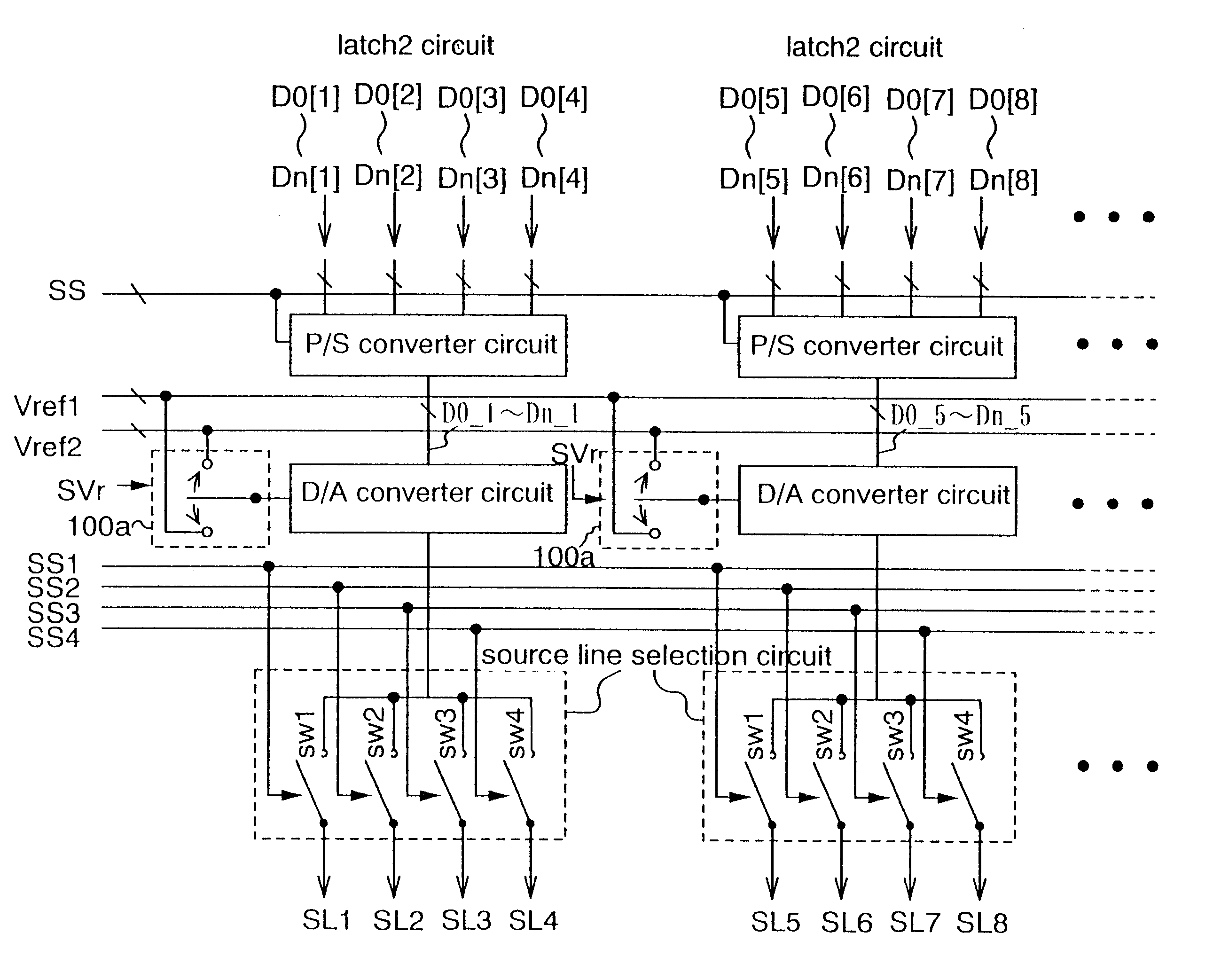
A circuit structure example of a source signal line driver circuit corresponding to embodiment mode 1 is shown in FIG. 13. Further, for convenience, an input digital image signal is taken as having three bits, and a case of driving four source signal lines by using one D / A converter circuit is explained.
Please refer to FIG. 13. A shift register portion has a flip-flop circuit FF, a NAND circuit, and an inverter, and a clock signal CLK, a clock signal CLKb which is an inverted clock signal CLK, and a start pulse SP are input. As shown in FIG. 14A, the flip-flop circuit FF is structured by a clocked inverter and an inverter.
When the...
embodiment 2
An active matrix liquid crystal display device is taken as a specific example of embodiment mode 2 and explained in embodiment 2. Further, the explanation below focuses on a source signal line driver circuit, similar to embodiment 1.
An example circuit structure of a source signal line driver circuit corresponding to embodiment mode 2 is shown in FIG. 18. Further, for convenience, an input digital image signal is taken as having three bits, and a case of driving three source signal lines by using one D / A converter circuit is explained.
Please refer to FIG. 18. A shift register portion, a latch 1 portion, and a latch 2 portion are the same as those of embodiment 1.
A 3 bit data.times.3 (a three source signal line portion) digital image signal stored in the latch 2 portion is input to a parallel / serial converter circuit (taken as a P / S converter circuit B in FIG. 18), along with externally input selection signals SS1 to SS3. The P / S converter circuit B is composed of NAND circuits, as sh...
embodiment 3
An active matrix liquid crystal display device is taken as a specific example of embodiment mode 3 and explained simply in embodiment 3.
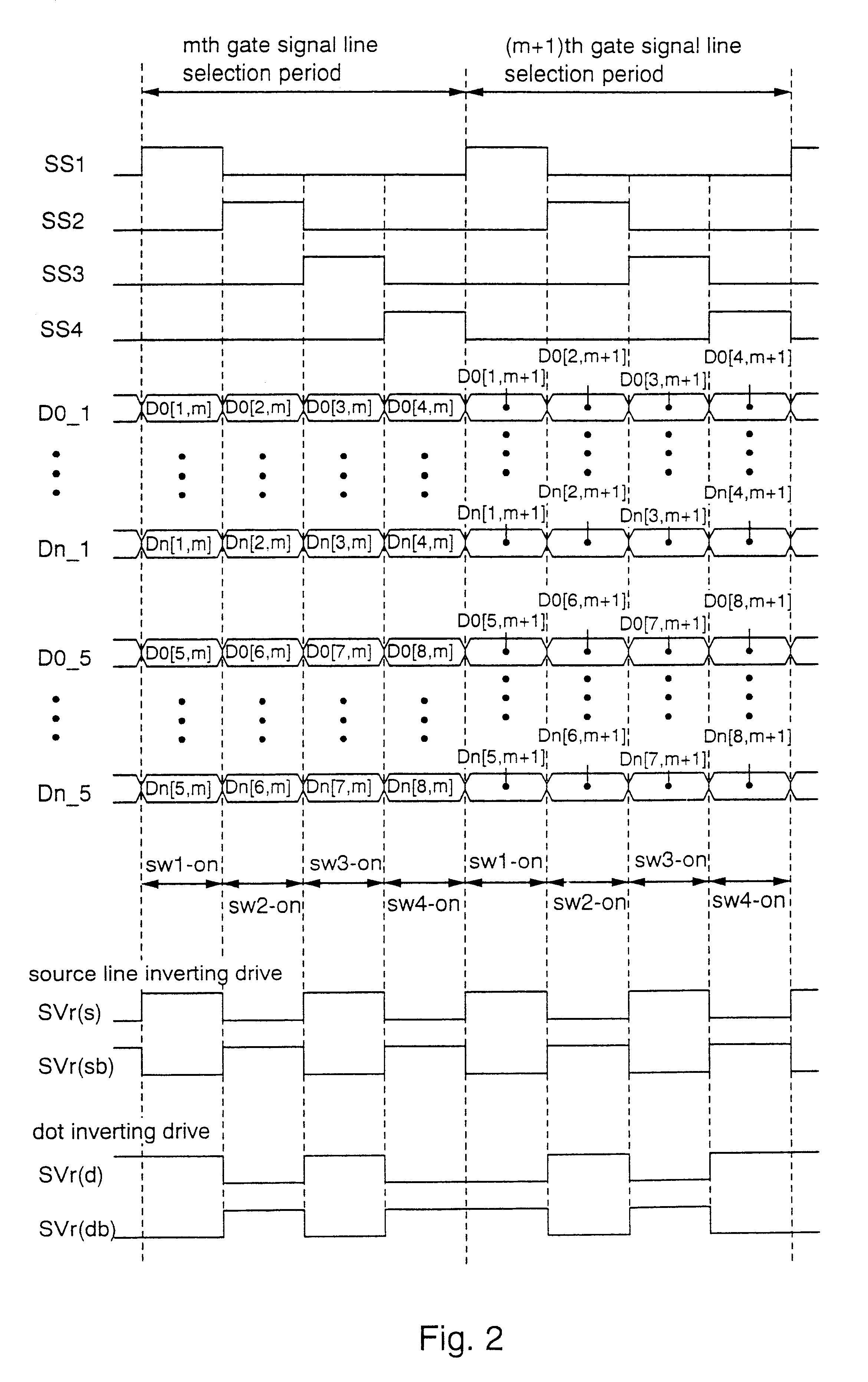
An example circuit structure of a source signal line driver circuit corresponding to embodiment mode 3 is the same as embodiment 1 and is shown in FIG. 13. What differs from embodiment 1 is a method of inputting selection signals SS1 to SS4 and a control signal SVr. The selection signals SS1 to SS4 as shown by FIG. 5 are input, and the control signal SVr may be input as SVr(s) and SVr(sb) when performing source line inverting drive, and as SVr(d) and SVr(db) when performing dot inverting drive.
PUM
 Abstract
Description
Claims
Application Information