Scanning tip and process for its production and use, particularly for a scanning probe microscope

a scanning probe and microscope technology, applied in scanning probe microscopy, nanotechnology, radiation therapy, etc., can solve the problems of not being able to produce scanning tips, requiring great care, and requiring rather complex production procedures, so as to achieve the effect of producing scanning tips and similar devices

Inactive Publication Date: 2004-07-27
NANOSURF +1
View PDF14 Cites 23 Cited by
  • Summary
  • Abstract
  • Description
  • Claims
  • Application Information

AI Technical Summary

Benefits of technology

As indicated above, the object of the present invention is to provide a method for producing scanning tips and similar devices which is easier, and thus more economical, than conventional production processes. The retrofitting of scanning tips onto existing structures shall be possible as well. Here, no compromises should be made in the quality of the scanning tips or their suitability for high resolution measuring. The particular advantage of the method is its possibility to laterally mount tips onto existing structures, i.e., on the same level as existing structures in a parallel process.
Thus, a particular advantage was not utilized at all by Genolet et al., namely that the processing of the photosensitive resist material can be performed in a normal environment, i.e. without a vacuum, highly clean room, or similar restrictions.
Another, rather general advantage is the enormously high technical standard of production processes presently achieved for microelectronics. This technology and the facilities required here are common and, thus can be reasonably purchased in high quality.
The invention can easily be adjusted to different conditions and can be modified in a simple manner. Therefore, it can be used for the production of scanning tips and for the mounting of additional tips onto a probe as well. On the other hand, the invention can also be used to produce or repair micromechanical sensors or probes that are used in other devices than scanning probe microscopes, e.g., in profile meters and measuring scanners. In the latter, an extremely small tip bending radius is not necessarily deciding, but frequently an optimally controlled geometry of the tip. This can easily be performed in the process according to the invention by embodying the mask accordingly, i.e. its shape and size, and, accordingly, by choosing the angle at which the exposure of the photo-structurable material occurs.
Due to the possibility of a lateral mounting at the cantilever, the tip can additionally be already mounted when the cantilever, together with a multitude of identical ones, is still "in situ" in the wafer, again allowing precise and inexpensive mass production.

Problems solved by technology

It is therefore obvious, that rather expensive processes for producing such scanning tips are being developed and great care is required in order to be able of producing the extremely small tip radius desired.
Frequently, the tips are integrated into other components of the microscope, in particularly embodied as parts of the probe, requiring rather complex production procedures.
This causes the production to be tedious and expensive.

Method used


Image

  • Scanning tip and process for its production and use, particularly for a scanning probe microscope
  • Scanning tip and process for its production and use, particularly for a scanning probe microscope

Examples


Embodiment Construction

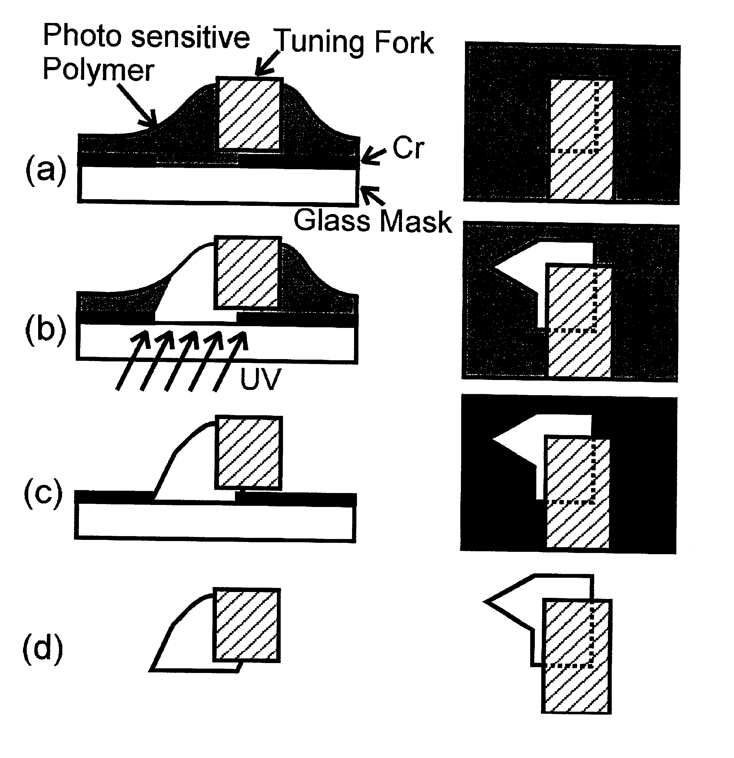
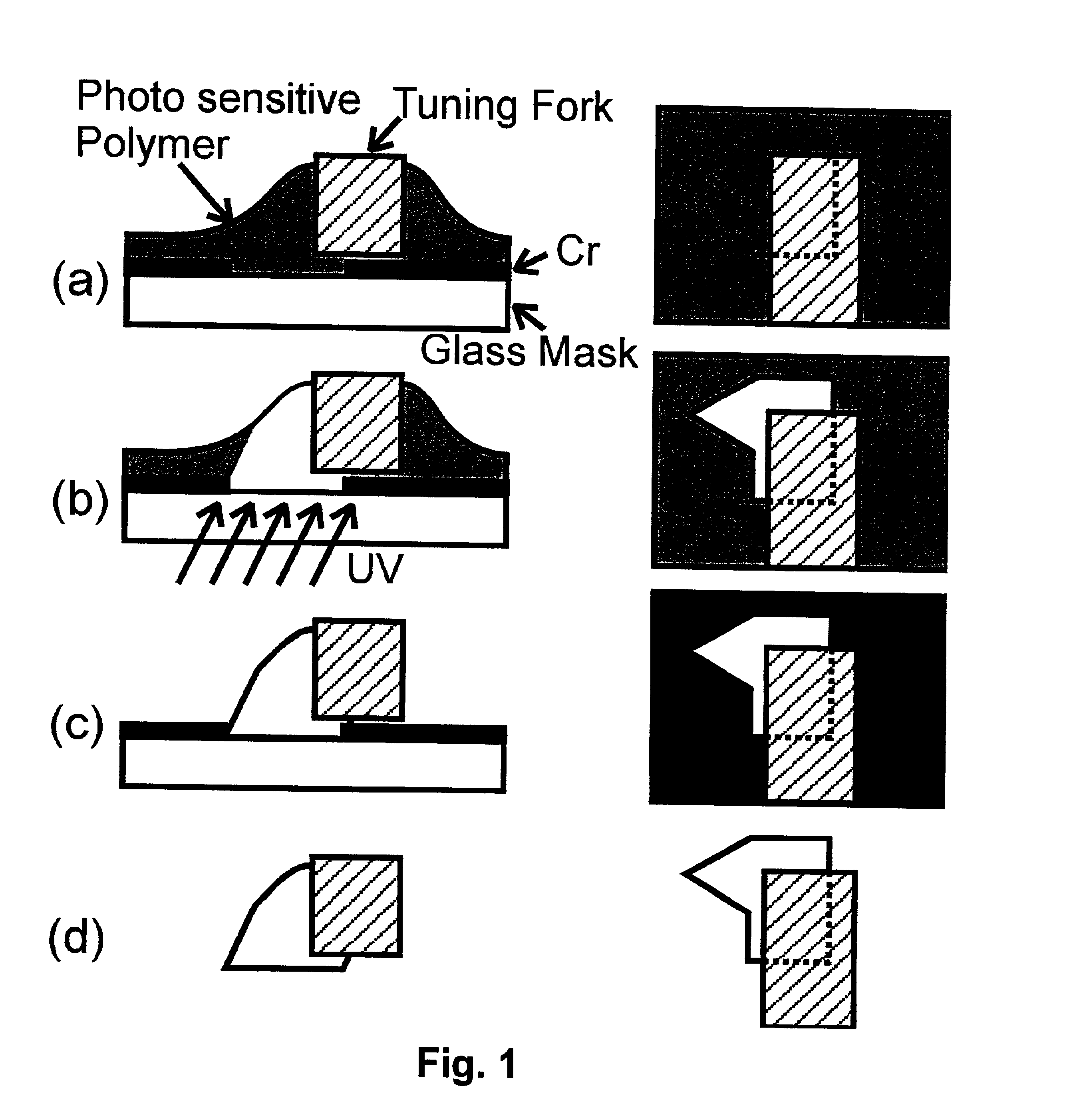
In the following, an exemplary embodiment of the invention is described in greater detail using the drawing in which FIGS. 1a-1d show various processing steps, and finally the result of these steps.

First the mask is prepared. As mentioned above, for the utilization in an AFM the bending radius of the scanning tip is the deciding quality criteria: the smaller, the better. The sharpness of the tip depends primarily on the measures and the layout of the masks used. A quartz mask is best suited for an optimal lithographic resolution. The best results were achieved in a square 5-inch mask, divided into four sections. This is called for since

a) the mask must be small to such an extent that it fits into the narrow space of the aligning device used, when the latter is tilted; and

b) this way, essentially four identical masks are produced in a single processing step.

The producer of the masks certifies an opening of 0.7 .mu.m on the most critical position or edge. This measurement should be as...


PUM


Abstract

The invention relates to so-called scanning tips of probes necessary for scanning a measured object, in particular in scanning force microscopes and other scanning microscopes, so-called scanning probe microscopes. The possible resolution of such microscopes depends primarily on the fineness of the tip, i.e. its curvature or radius being as small as possible. According to the invention, a photostructurable material, e.g. a photosensitive resists, serves as the material for the scanning tip which is exposed via a mask and is subsequently developed / hardened in a manner known per se. The unexposed parts of the photosensitive resist are removed as usual. By the shape of the exposure mask, the preferably directed exposure of the photosensitive resist, and the subsequent hardening, a tip is formed preferably laterally on or at a carrier, usually made from a different material, which is provided with a very small radius, thus very well suitable for scanning probe microscopy and similar applications. By an appropriate selection of the mask and / or the exposure angle, the geometry of the tip can be controlled, in particular its bending radius and edge angle, for other applications as well, e.g. for measuring scanners or profile meters.

Description

The invention relates to so-called scanning tips in probes for scanning a measured object as are in particular necessary for scanning force microscopes and other scanning microscopes, so-called scanning probe microscopes. In such microscopes, the achievable resolution is primarily dependent on the fineness of the tip, i.e. the curvature or radius of the outermost tip being as small as possible. In detail, the invention relates to a novel method for producing such scanning tips, probes having scanning tips produced according to said method, and, finally, the use of such scanning tips in a scanning probe microscope.PRIOR ARTIn scanning probe microscopy, a scanning tip commonly picks up the interaction of a probe and a measured object, i.e. a specimen, and leads the result to a suitable electronic. For scanning the specimen, essentially two methods are used. On the one hand, the so-called static mode in which the probe is mounted on an oscillating beam or cantilever and is in a fine co...

Claims


Application Information

Patent Timeline
Patent Type & Authority Patents(United States)
IPC IPC(8): G21K7/00G01Q70/14G01Q70/16
CPCB82Y35/00G01Q70/14G01Q70/16Y10S977/879
Inventor HOWALD, LUKASSCANDELLA, LORISSTAUFER, URSAKIYAMA, TERUNOBU
Owner NANOSURF
Why Eureka
Try Eureka