

Analog-to-digital conversion method and device
a conversion method and digital data technology, applied in the field of analog-to-digital (a/d) conversion methods and devices, can solve the problems of system insufficient speed, quantity of variation of analog input signals cannot be reflected on the resultant digital data, and system cannot meet the requirement for high-speed a/d conversion
- Summary
- Abstract
- Description
- Claims
- Application Information
AI Technical Summary
Benefits of technology
Problems solved by technology
Method used
Image

Examples
second example
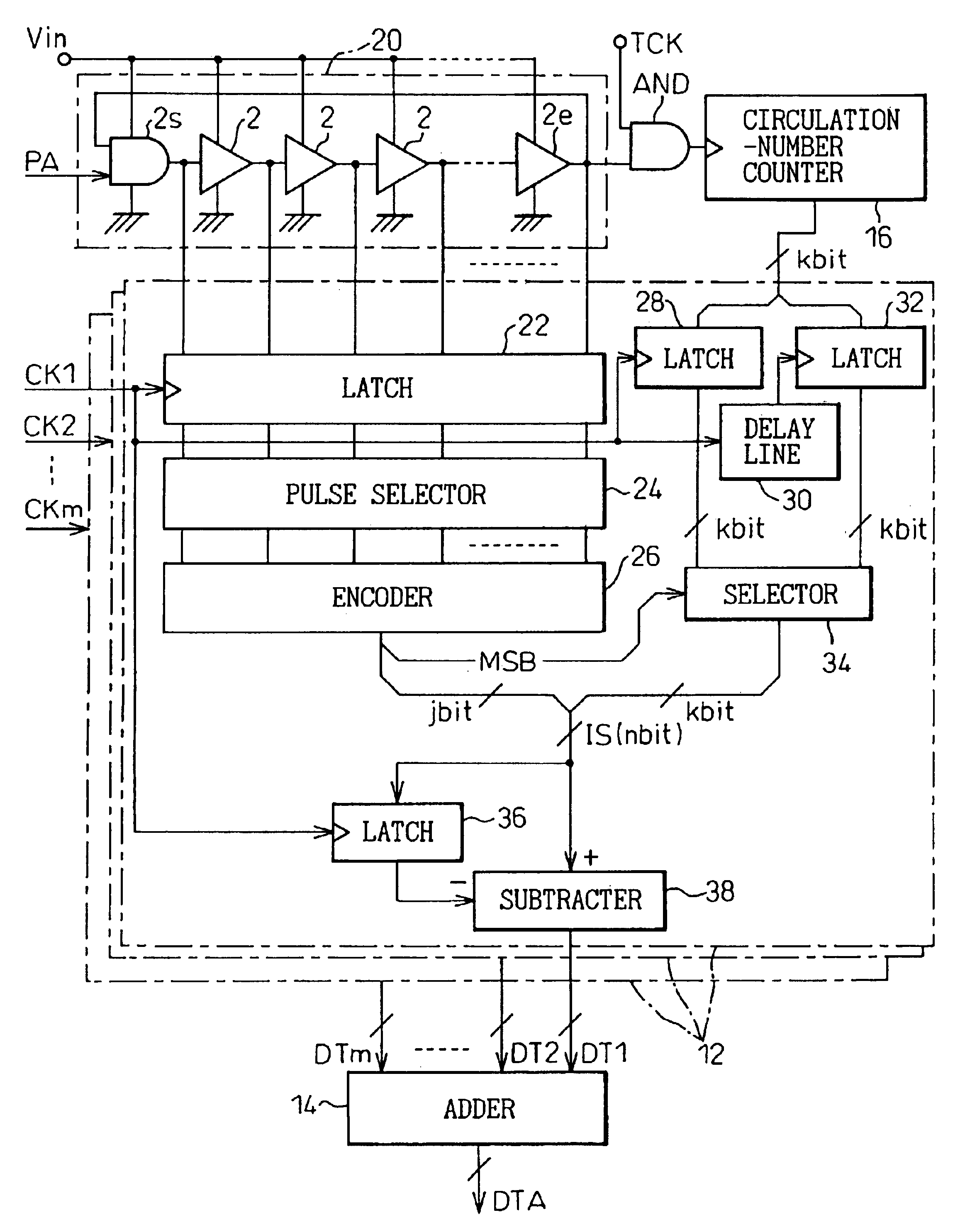
Next, FIG. 4 is a block diagram showing the configuration of an A / D conversion device of a second example to which the present invention (or more particularly, any of the first to tenth embodiments) is adapted.
The A / D conversion device of the second example shown in FIG. 4 includes a pulse circulation circuit 20 instead of the pulse delay circuit 10 included in the first example. The pulse circulation circuit 20 has delay units 2 concatenated annularly so that a pulse signal PA can be returned from a delay unit 2e of a final stage to a delay unit 2s of an initial stage for the purpose of circulating the pulsating signal. An output of the delay unit 2s of the final stage in the pulse circulation circuit 20 is applied to a circulation-number counter 16 via an AND circuit AND. The circulation-number counter 16 then counts the number of times by which the pulse signal has circulated through the pulse circulation circuit 20.
The A / D conversion device of the second example includes, simila...
first embodiment
The AND circuit AND located on a pulsating signal input path along which a pulse signal is transmitted from the pulse circulation circuit 20 to the circulation-number counter 16 corresponds to the input circuit included in the twenty- When an input terminal of the AND circuit that is not connected to the delay unit 2e of the final stage in the pulse circulation circuit 20 is high, an output of the delay unit 2e is applied to the circulation-number counter 16. The counting action of the circulation-number counter 16 is thus enabled. In contrast, when the output of the delay unit 2e of the final stage is low with the circulating action of the pulse circulation circuit 20 stopped, a test clock TCK for use in testing the counter is applied to the input terminal of the AND circuit that is not connected to the delay unit 2e of the final stage. Thus, the counting action of the circulation-number counter 16 can be tested.
In the A / D conversion device of the present example having the foregoi...
third example
FIG. 9 is a block diagram showing the configuration of an A / D conversion device of a third example to which the present invention (more particularly, any of the first to tenth embodiments of the present invention) is adapted.
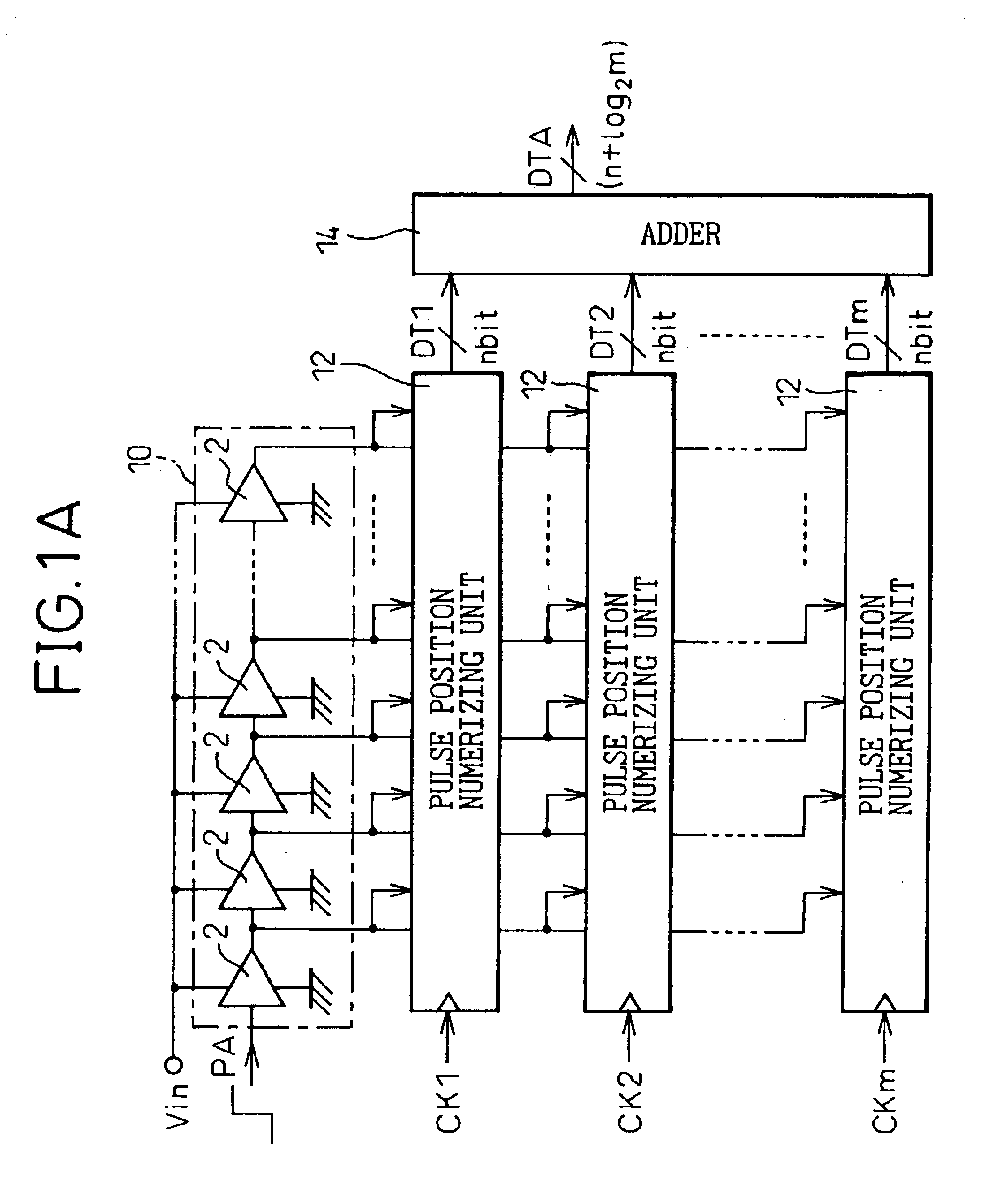
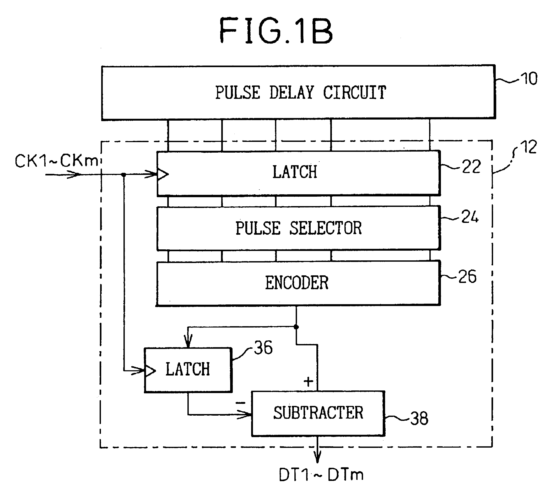
The A / D conversion device of the present example has the same components as the A / D conversion device of the first example and can achieve A / D conversion with higher precision. The A / D conversion device has a pulse delay circuit 10, four pulse position numerizing units 12, and an adder 14 which have the same configurations as those included in the A / D conversion device of the first example.
Latches 13a to 13d that latch numerical data synchronously with a reference clock CK0, which is applied externally for A / D conversion, are located on input paths along which numerical data is transmitted from the pulse position numerizing units 12 to the adder. Sampling clocks CK1 to CK4 are transmitted to the respective pulse position numerizing units 12 via a sampling clock ...
PUM
 Abstract
Description
Claims
Application Information