Optical device

a technology of optical devices and optical waveguides, applied in the direction of optical waveguide light guides, instruments, nanotechnology, etc., can solve the problem of complex structur

Inactive Publication Date: 2004-11-02
PANASONIC CORP
View PDF18 Cites 26 Cited by
  • Summary
  • Abstract
  • Description
  • Claims
  • Application Information

AI Technical Summary

Benefits of technology

In order to achieve the object of the present invention, an optical device (CL1) according to the present invention includes a first optical member separating an incident light of wavelength .lambda. into TE wave and TM wave; and an optical input portion, which inputs the incident light into the first optical member; wherein the first optical member has a periodically changing refractive index; wherein an angle defined by a first reciprocal lattice vector .alpha..sub.1 and a second reciprocal lattice vector .alpha..sub.2 of the first optical member at the wavelength .lambda. is not larger than 90.degree.; wherein, in the direction of the first reciprocal lattice vector .alpha..sub.1, the wave number of the TE wave is larger than the wave number of the TM wave; wherein, in the direction of the second reciprocal lattice vector .alpha..sub.2, the wave number of the TE wave is smaller than the wave number of the TM wave; and wherein the optical input portion inputs the incident light in a direction that is parallel to a plane P.sub.12 including the first reciprocal lattice vector .alpha..sub.1 and the second reciprocal lattice vector .alpha..sub.2. With this optical device, the difference between the dispersion surfaces of the TE waves and the TM waves in the demultiplexing portion becomes large, and the separation angle of the TE waves and the TM waves can be set to be large. As a result, it is possible to separate TE waves and TM waves at a propagation distance at which the influence of diffraction can be ignored, and it is possible to reduce the number of optical parts, such as lenses, and to make the device smaller.

Problems solved by technology

Such an optical isolator reflects light that is incident light from the light-source side, so that a separate optical system or optical design is necessary to make sure that the reflected light is not coupled into the light-source side, which makes the structure more complicated.

Method used


Image

  • Optical device
  • Optical device
  • Optical device

Examples


embodiment 1

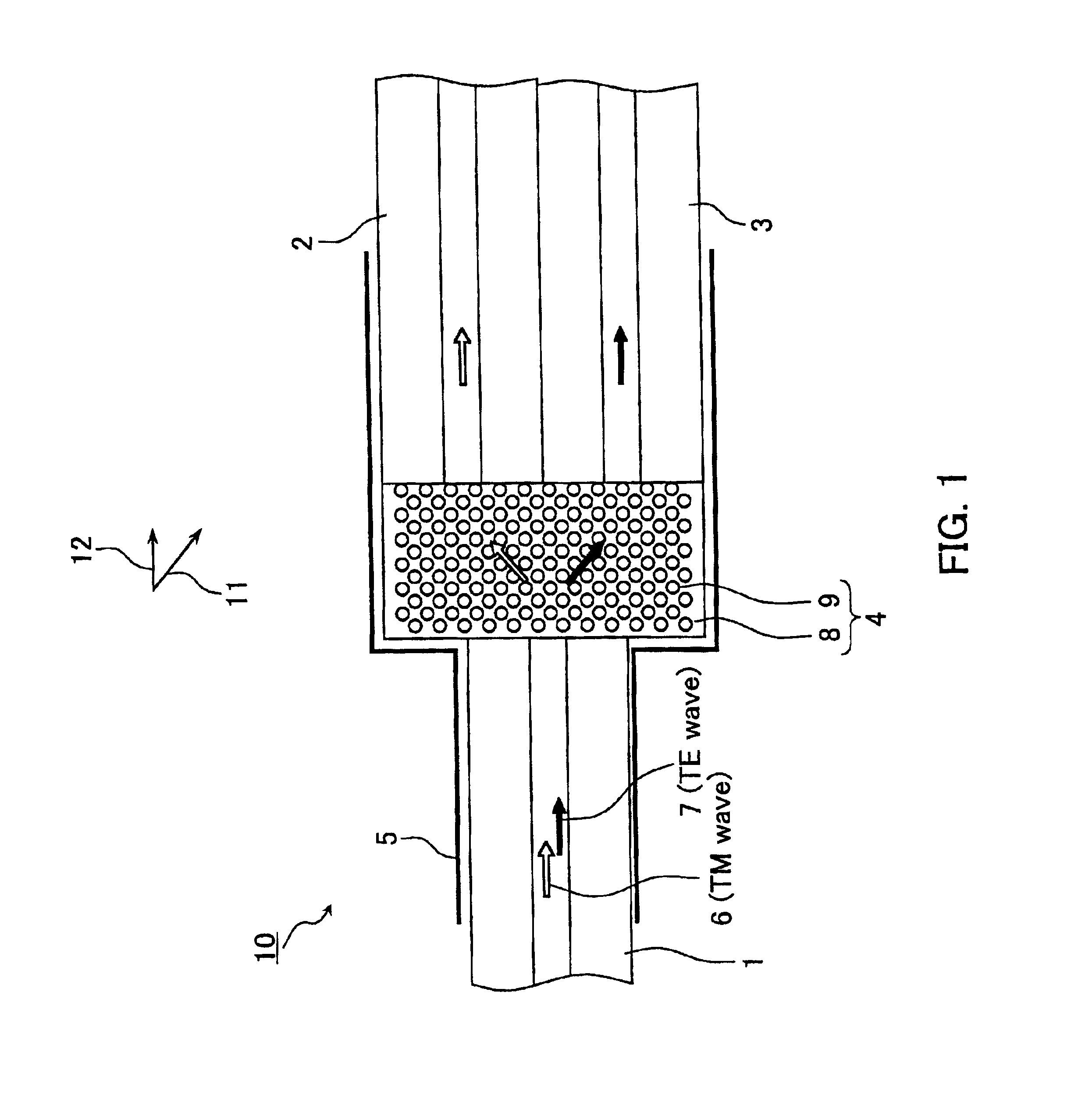
Embodiment 1 illustrates a demultiplexer as an example of an optical device according to the present invention. FIG. 1 schematically illustrates the configuration of an optical device 10 according to Embodiment 1. It should be noted that hatching lines have been omitted from Figures.

The optical device 10 includes an optical fiber 1 (F(0)) on the ingoing side, optical fibers 2 and 3 (F(1) and F(2)) on the outgoing side, a demultiplexing portion 4, and a guide 5. The guide 5 fixes the relative positions of the optical fibers 1 to 3 and the demultiplexing portion 4. The optical fibers 1 to 3 each include a core portion through which light propagates, and a cladding portion disposed around the core portion.

The demultiplexing portion 4 (also referred to as "first demultiplexing portion 4" in the following embodiments) is an optical member (first optical member) separating incident light of a wavelength .lambda. into a TE wave (ordinary light) and a TM wave (extraordinary light). The demu...

embodiment 2

Embodiment 2 illustrates a demultiplexer as an example of an optical device according to the present invention. FIG. 5A schematically illustrates the configuration of an optical device 50 of Embodiment 2. FIG. 5B illustrates the polarization state of the light emitted from the various optical components.

The optical device 50 includes an ingoing optical fiber 1, outgoing optical fibers 51 to 54, a first demultiplexing portion 4 (first optical member), a second demultiplexing portion 56 (second optical member), and a guide 57. The guide 57 fixes the relative positions of the optical fiber 1, the first demultiplexing portion 4, the second demultiplexing portion 56, and the optical fibers 51 to 54. The first demultiplexing portion 4, the second demultiplexing portion 56, and the optical fibers 51 to 54 are arranged such that light that is inputted by the optical fiber 1 is transmitted in that order.

The first demultiplexing portion 4 and the second demultiplexing portion 56 are optical m...

embodiment 3

Embodiment 3 illustrates a demultiplexer as an example of an optical device according to the present invention. FIG. 6A schematically illustrates the configuration of an optical device 60 of Embodiment 3. FIG. 6B illustrates the polarization state of the light emitted from the various optical components.

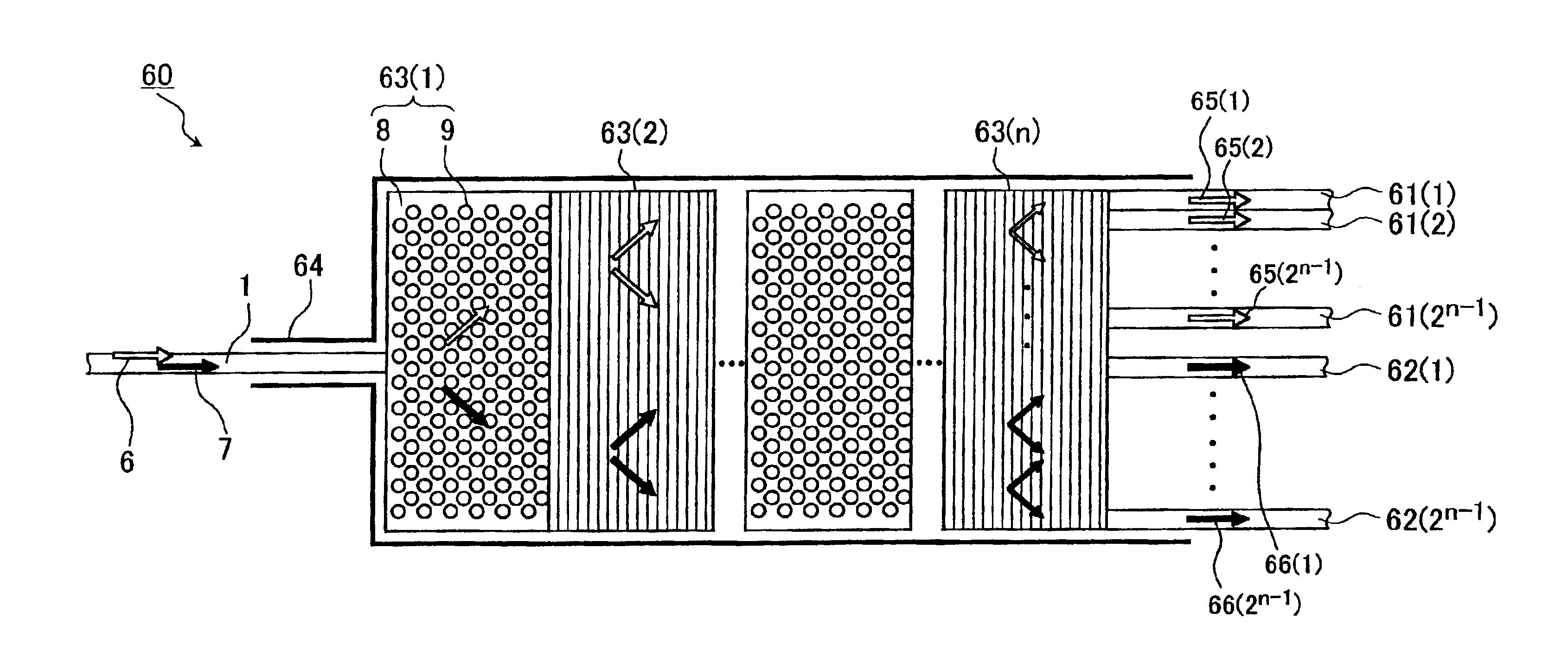
The optical device 60 is a 2n demultiplexer. The optical device 60 includes an ingoing optical fiber 1, outgoing optical fibers 61(1) to 61(2.sup.n-1) and 62(1) to 62(2.sup.n-1), n demultiplexing portions 63(1) to 63(n), and a guide 64. The guide 64 fixes the relative positions of the optical fiber 1, the optical fibers 61 and 62, and the demultiplexing portions 63.

The n demultiplexing portions 63(1) to 63(n) are optical members having a structure similar to the demultiplexing portion 4 in Embodiment 1. That is to say, these optical members include a first material 8 having an ingoing plane and an outgoing plane that are parallel to one another, and columnar portions 9 arranged insid...


PUM

PropertyMeasurementUnit
wavelengthaaaaaaaaaa
separation angleaaaaaaaaaa

Abstract

The invention provides a small optical device with which incident light can be demultiplexed. The optical device includes a demultiplexing portion 4 (first optical member) separating TE waves and TM waves of incident light of a wavelength lambda and an optical fiber 1 (optical input portion) inputting incident light into the demultiplexing portion 4. The demultiplexing portion 4 has a periodically changing refractive index. The angle defined by the first reciprocal lattice vector alpha1 and the second reciprocal lattice vector alpha2 of the demultiplexing portion 4 at the wavelength lambda is not greater than 90°. In the direction of the first reciprocal lattice vector alpha1 the wave number of the TE wave is larger than the wave number of the TM wave. In the direction of the second reciprocal lattice vector alpha2 the wave number of the TE wave is smaller than the wave number of the TM wave. The optical fiber 1 inputs the incident light in a direction that is parallel to a plane including the first reciprocal lattice vector alpha1 and the second reciprocal lattice vector alpha2.

Description

1. Field of the InventionThe present invention relates to optical devices, and more particularly, to optical devices such as optical interleavers and polarization-dependent optical isolators used for WDM (wavelength division multiplexing) optical communication.2. Related Background ArtFIG. 21 shows an example of a conventional optical demultiplexer 900 made of a natural birefringent material, such as rutile. The demultiplexer 900 includes an ingoing optical fiber 901, an ingoing lens 902, a birefringent material 903 such as rutile, a first outgoing lens 904, a first outgoing optical fiber 905, a second outgoing lens 906, and a second outgoing optical fiber 907. Incident light that is coupled from the ingoing optical fiber 901 through the ingoing lens 902 into the birefringent material 903 is separated into ordinary light (TE wave) 909 and extraordinary light (TM wave) 908. The ordinary light 909 and the extraordinary light 908, which are separated by a distance proportional to the l...

Claims


Application Information

Patent Timeline
Patent Type & Authority Patents(United States)
IPC IPC(8): G02F1/09G02F1/01G02B6/122G02B6/12G02B6/126
CPCB82Y20/00G02B6/12007G02B6/1225G02F1/093G02B6/126G02F2203/06G02B2006/12157G02F2202/32
Inventor HAMADA, HIDENOBU
Owner PANASONIC CORP
Why Eureka
Try Eureka