Method of manufacturing image forming apparatus

a technology of image forming apparatus and manufacturing method, which is applied in the direction of lighting and heating apparatus, tube/lamp factory adjustment, instruments, etc., can solve the problems of unrealistic long process and insufficient uniformity, and achieve the effect of reducing low electric field strength, large electric field strength and lessening electric field strength

Inactive Publication Date: 2004-11-23
CANON KK
View PDF16 Cites 41 Cited by
  • Summary
  • Abstract
  • Description
  • Claims
  • Application Information

AI Technical Summary

Benefits of technology

Inventors of the present invention found, in advance of a normal drive in a manufacturing process, that variation over time can be reduced by carrying out a preliminary drive processing.
In addition, in this embodiment, the procedure was that the characteristic adjustment look-up table is prepared with respect to each display panel 301, and on the basis of the characteristic adjustment look-up table, the characteristic adjustment is carried out. However, in this embodiment and a second embodiment which will be described later, in case that the characteristic adjustment is carried out by setting the luminance target values L0 of the emitters to the same values in the display panels 301 of the same lot, the characteristic adjustment look-up table is prepared only for the first one piece of the display panel, and in display panels of a second one and thereafter, if the measurement result of the electron emission characteristic at the time of application of the normal drive voltage Vdrv after the preliminary drive voltage Vpre is applied to all SCE-emitters of the display panel 301 is in a range of being capable of setting to the luminance target value L0 of the SCE-emitter, even if the characteristic variation curves shown in FIG. 6 or FIG. 10 is not obtained, it is possible to carry out the characteristic adjustment by use of the characteristic adjustment look-up table of the first one piece of the display panel, and it is possible to reduce processing time of the characteristic adjustment process to display panels of the second one and thereafter.

Problems solved by technology

Also, It is possible that, due to this occurrence of the variation of adjustment situations, the characteristic shift voltage was applied excessively so that the characteristic becomes of a value less than the standard value, and the characteristic was not shifted up to the standard value even after the characteristic shift voltage was applied only for a desired time period, which means that uniformity is not sufficiently improved.
Furthermore, there was a case that, when an identical amplitude is applied with respect to each emitter, shift amount is smaller than estimated amount in advance, and the time required until the characteristic is shifted to a target value is lengthened so that the process becomes a unrealistic lengthy process.

Method used


Image

  • Method of manufacturing image forming apparatus
  • Method of manufacturing image forming apparatus
  • Method of manufacturing image forming apparatus

Examples


first embodiment

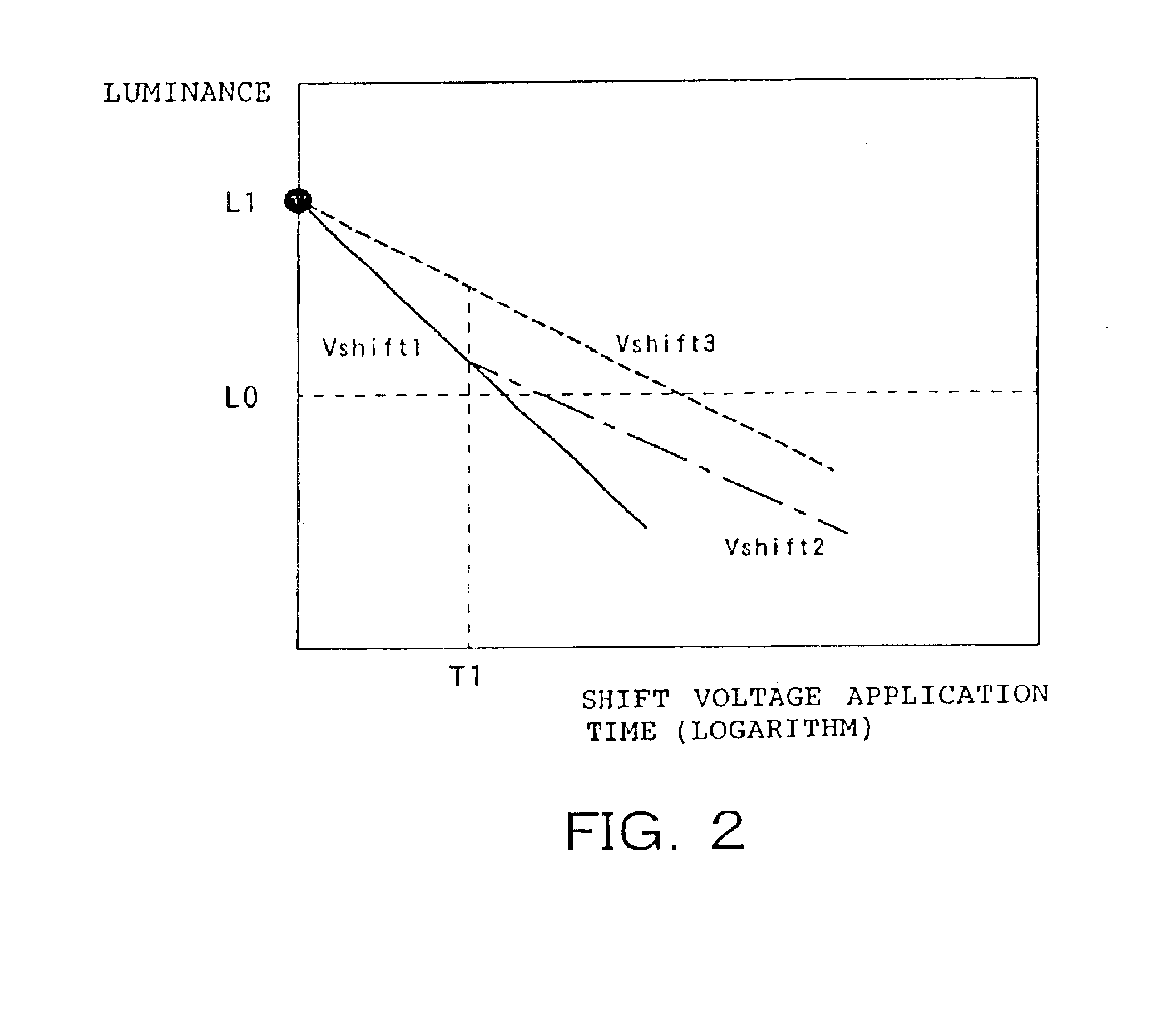
Firstly, as described in the first embodiment, the luminance target value L0 is determined on the basis of the average luminance and the standard deviation.

In this example, the target luminance L0 is set at 9600 (a.u.). In addition, the value of the luminance is a value which corresponds to the luminance obtained from CCD.

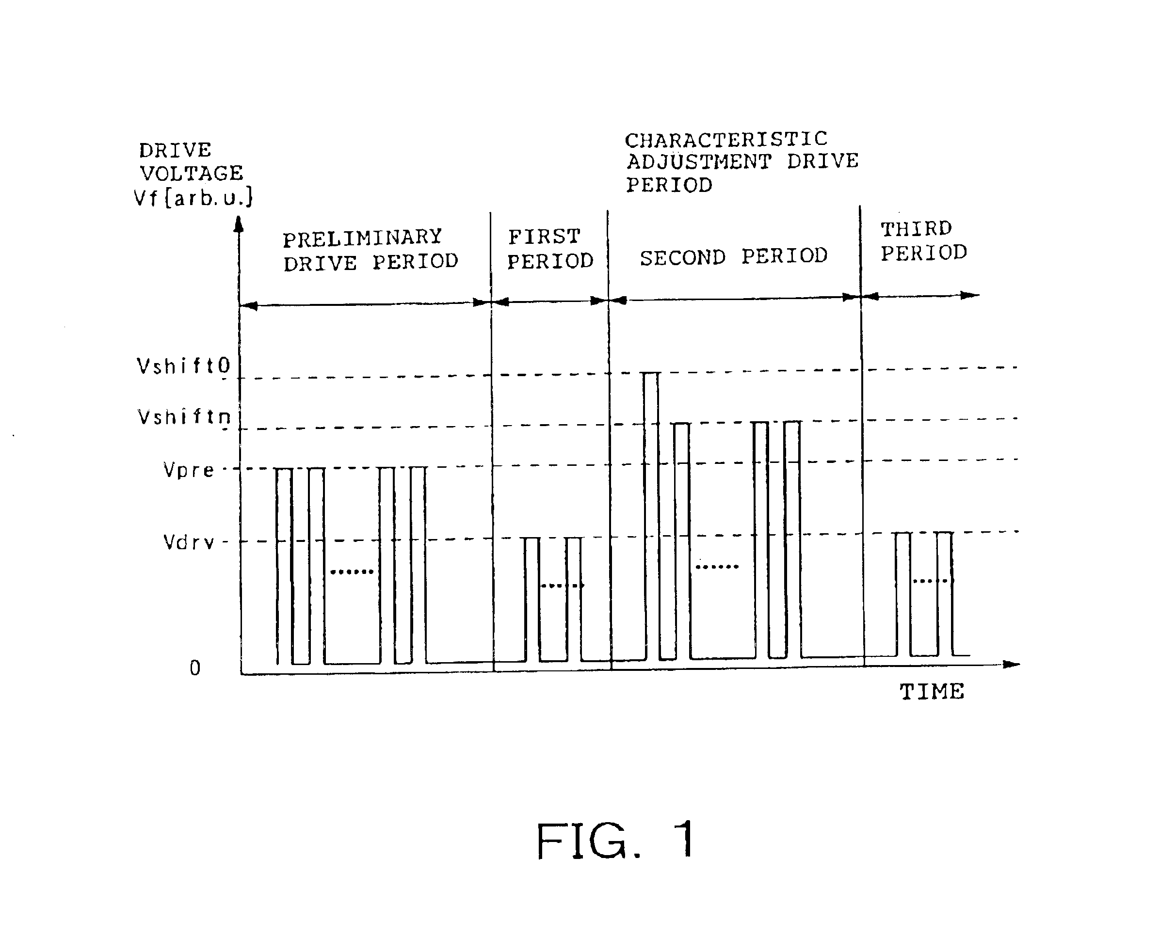
Next, pulse width is set to 1 msec, and cycle is set to 10 msec, and others are set to satisfy Vpre=16V, Vdrv=14.5V, Vshift1=16.5V, Vshift2=17V, Vshift3=17.5V, Vshift4=18V, Vshift1'=16V, Vshift2'=16.5V, and Vshift3'=17V. And, as described in the first embodiment, the look-up table was prepared.

Hereinafter, procedures of characteristic adjustment method will be described by use of a flow chart of FIG. 7.

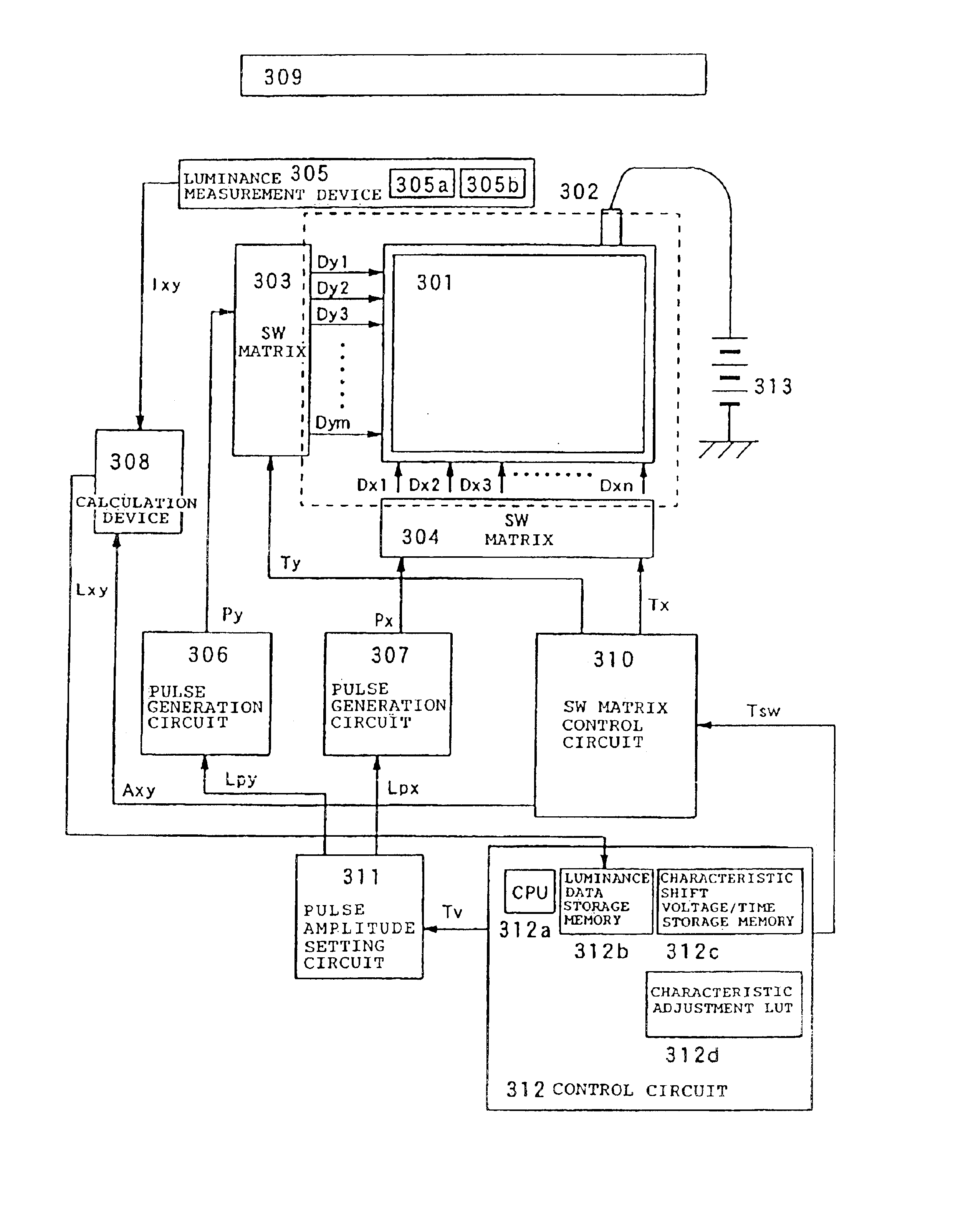
Firstly, at Step S1, set is the number of applied pulses which are applied at the time of characteristic adjustment to one of SCE-emitters to which the characteristic adjustment is carried out in the display panel 301. The number of applied pulses is set to 10 pulses...

example 2

As described above, there exist a small number of electron sources in which rates of changes to the number of applied pulses in the characteristic variation curves shown in FIG. 6 differ greatly. In this example, even as to such electron sources, by incorporating a way, described later, of coping with them into the steps (1) and (2) for adjusting the characteristic of large majority of the electron sources, it became possible to adjust the characteristic thereof.

Here, a method of setting characteristic shift voltages and a method of adjusting characteristics which are different from those of the example 1 will be described. As to other processes, similar techniques to the example 1 were used and therefore, descriptions thereof will be omitted. Also, SCE-emitters used and voltage setting were made to be the same as the example 1. Further, the luminance target value L0 is also set at 9600 (a.u).

As the electron source which did not reach the vicinity of the target luminance regardless ...

example 3

In this example, correction of the characteristic voltage which was carried out in the example 2 was carried out with respect to each pulse. Here, a method of setting characteristic shift voltages and a method of adjusting characteristics which are different from those of the example 1 will be described. As to other processes, similar techniques to the example 1 were used and therefore, descriptions thereof will be omitted.

Compared are shift amount calculated from luminance Lp (before application) and Lp' (after application) at the time of applying Vdrv before and after the characteristic shift voltage pulse is applied and shift amount which was estimated. Assuming that the estimated shift amount is Dn, actual shift amount Dr becomes Dr=L1' / L1, from the luminance Lp before the application of one pulse of the characteristic shift voltage and luminance L1' after that.

A difference .DELTA.D of the shift amounts is described as .DELTA.D=Dn-Dr.

Thereby, it has been found that, in case of ....


PUM


Abstract

The present invention relates to the adjustment of luminance. The present invention is a method of manufacturing image forming apparatus including a step of applying characteristic shift voltage comprising a plurality of pulses in which the amplitude of the pulse obtained from the look-up table has two or more values, to the emitter, the look-up table storing the amplitude of the pulse and the number of the pulse for shifting characteristic of emitters to a predetermined luminance target value on the basis of the measurement result of the luminance. Moreover, the present invention is a method of manufacturing image forming apparatus comprising a step of applying the second pulses of characteristic shift voltage having the amplitude which was determined in response to the measurement result of the luminance after the first characteristic shift voltage had been applied to the emitter.

Description

This application claims the right of priority under 35 U.S.C. .sctn. 119 based on Japanese Patent Application Nos. JP 2002-1358, filed on May 8, 2002, and JP 2003-124208, filed on Apr. 28, 2003 which are hereby incorporated by reference herein in their entirety as if fully set forth herein.1. Field of the InventionThis invention relates to a method of manufacturing an image forming apparatus with a multiple electron source comprising a number of electron emitters.2. Description of the Related ArtConventionally, as a method of suppressing variation of electron emission characteristics of individual electron emitters constituting the multiple electron source, known is a method of adjusting a characteristic disclosed in JP-A-10-228867 (Literature 1) and JP-A-2000-243256 (Literature 2).In the literature 1, disclosed is a fact that, in a multiple electron source in which Surface Conduction Electron Emitters (hereafter, represented by SCE-emitter) are arranged in a matrix, voltage to be m...

Claims


Application Information

Patent Timeline
Patent Type & Authority Patents(United States)
IPC IPC(8): G09G3/00G09G3/22H01J9/44
CPCG09G3/006G09G3/22G09G2320/0693G09G2320/0285H01J9/42
Inventor KAWASAKI, HIDESHIAOKI, SHUJITABATA, IZUMIYAMANO, AKIHIKOSAKATA, HISASHI
Owner CANON KK
Why Eureka
Try Eureka