Chalcogenide memory device with multiple bits per cell

a memory device and chip technology, applied in semiconductor devices, digital storage, instruments, etc., can solve the problem of insufficient memory density, and achieve the effect of reducing the required energy inpu

Inactive Publication Date: 2005-01-04
MACRONIX INT CO LTD
View PDF6 Cites 162 Cited by
  • Summary
  • Abstract
  • Description
  • Claims
  • Application Information

AI Technical Summary

Benefits of technology

Another object of the present invention is to provide an energy-saving chalcogenide memory. The contact area between the chalocogenide layer and electrode is controlled by the thickness of the diode. Thus, the contact area is reduced to a minimum dimension below the photolithographic limit. This can reduce the required energy input to the chalcogenide active region in operation.

Problems solved by technology

However, the conventional chalcogenide memory can store only one bit on one cell, thus, the memory density is not sufficient.

Method used


Image

  • Chalcogenide memory device with multiple bits per cell
  • Chalcogenide memory device with multiple bits per cell
  • Chalcogenide memory device with multiple bits per cell

Examples


Embodiment Construction

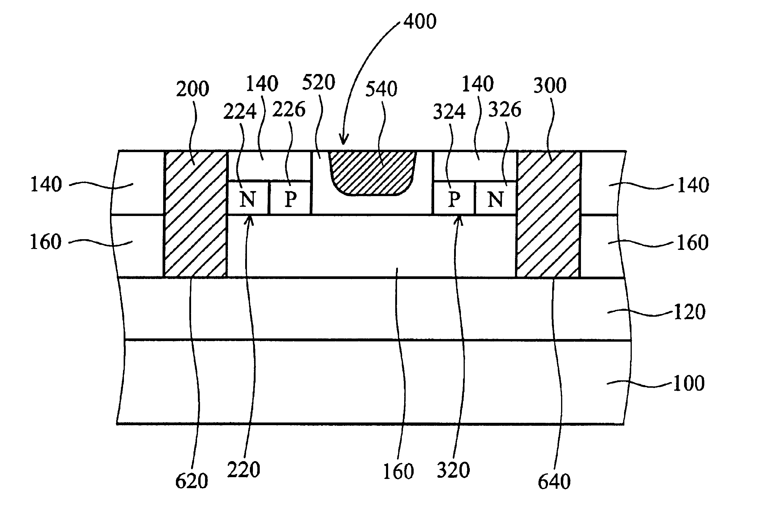
FIG. 3h shows a cross-section of a chalcogenide memory according to an embodiment of the present invention. Symbol 100 refers to a semiconductor substrate, and symbol 120 a conductive layer, for example, a polysilicon or tungsten word line. A memory device, including a first side electrode 200, a second side electrode 300, and a storage region 400, is formed on the word line 120. A dielectric layer 160 is disposed on the word line 120 to isolate the word line 120 and storage region 400.

The first side electrodes 200 and 300 can be made of metal, for example, a tungsten plug. The storage region 400 is laterally disposed between the first and second side electrodes 200 and 300. The storage region 400 includes a first doped semiconductor region 220, a second doped semiconductor region 320, a layer of phase-changing material 520, and an upper electrode 540.

The first doped semiconductor region 220 is disposed laterally in contact with a sidewall of the first side electrode 200. Also, the ...


PUM


Abstract

A memory device with multiple bits per-cell. The memory device includes a side electrode; a doped semiconductor region disposed laterally in contact with a sidewall of the side electrode, such that the doped semiconductor region forms a diode, or the junction between the side electrode and the doped semiconductor region forms a diode; a layer of phase-changing material disposed laterally in contact with a sidewall of the doped semiconductor region, such that the doped semiconductor region is disposed between the layer of phase-changing material and the side electrode; and an upper electrode disposed on the layer of phase-changing material. Many storage regions can be stacked vertically, and multiple bits can be stored in one cell. Also, the contact area is reduced to a minimum dimension below the photolithographic limit.

Description

BACKGROUND OF THE INVENTION1. Field of the InventionThe present invention relates to a chalcogenide memory device, and more particularly to a chalcogenide memory device with multiple bits per cell.2. Description of the Prior ArtThe use of chalcogenide material in memory devices is well known in the art. For example, Ovshinsky et al. in U.S. Pat. No. 5,296,716 disclose the use of chalcogenide materials and provide a discussion of the current theory of operation of chalcogenide materials.Chalcogenide material can be electrically switched between amorphous and crystalline states and exhibits different electrical characteristics depending upon its state. For example, in its amorphous state, the material exhibits lower electrical conductivity than it does in its crystalline state. Because chalcogenide material retains its programmed state even after removal of the electrical stimulus, chalcogenide memories are non-volatile. As an added benefit, chalcogenide elements may be programmed int...

Claims


Application Information

Patent Timeline
Patent Type & Authority Patents(United States)
IPC IPC(8): G11C11/56H01L27/24
CPCG11C11/56G11C11/5678H01L27/2409H01L27/2481G11C13/0004G11C2213/71H01L45/122H01L45/144H01L45/1666H01L45/06H10B63/84H10B63/20H10N70/821H10N70/231H10N70/8828H10N70/061
Inventor LUNG, HSIANG-LAN
Owner MACRONIX INT CO LTD
Why Eureka
Try Eureka