Flash memory device and method of erasing the same

a flash memory and eraser technology, applied in static storage, digital storage, instruments, etc., can solve the problems of increasing the erase time, reducing the erase and reduction of the sensing margin in the memory cell, and reducing the erase time to the sum of the time taken, so as to simplify the state machine circuit

Inactive Publication Date: 2005-01-11
SK HYNIX INC
View PDF7 Cites 48 Cited by
  • Summary
  • Abstract
  • Description
  • Claims
  • Application Information

AI Technical Summary

Benefits of technology

[0020]The present invention is contrived to solve the above problems and an object of the present invention is to provide a flash memory device capab

Problems solved by technology

First, as the bias voltages applied upon the program (or erase) and verify operations that are iteratively performed in each of the steps (first step˜third step) are different in the erase operation, it is required that operations for setting the bias voltages corresponding to the respective steps (first step˜third step) be iteratively performed. Due to this, the operation time for setting the bias voltage is accumulated during the entire erase operation. In particular, time consumed in the pre-program and post-program steps is almost same to time consumed in an actual erase step due to accumulated operating time for setting the bias voltage, thus increasing the erase time.
Second, in the conventional erase operation, time taken to apply the bias voltages in the respective steps (first step˜third step) is fixed to the allocated time (e.g. specific time). The bias voltages are continuously applied to the corresponding memory cells during remaining time even though the corresponding memory cells are controlled to the threshold voltages during the allocated time. Due to this, as the t

Method used


Image

  • Flash memory device and method of erasing the same
  • Flash memory device and method of erasing the same
  • Flash memory device and method of erasing the same

Examples


Embodiment Construction

sent invention will be explained in the following description, taken in conjunction with the accompanying drawings, wherein:

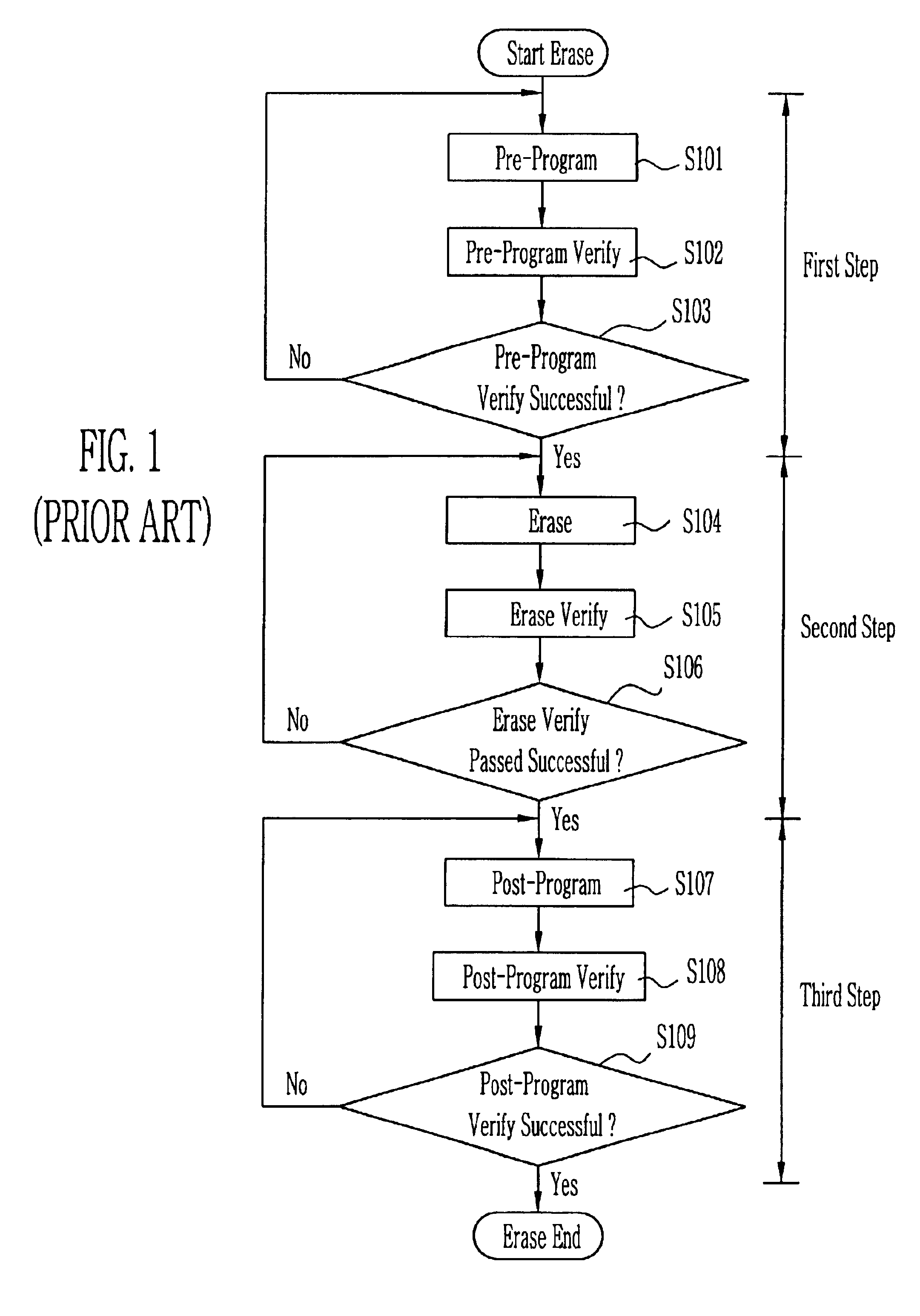
[0026]FIG. 1 is a flowchart for explaining a conventional method of erasing a flash memory device;

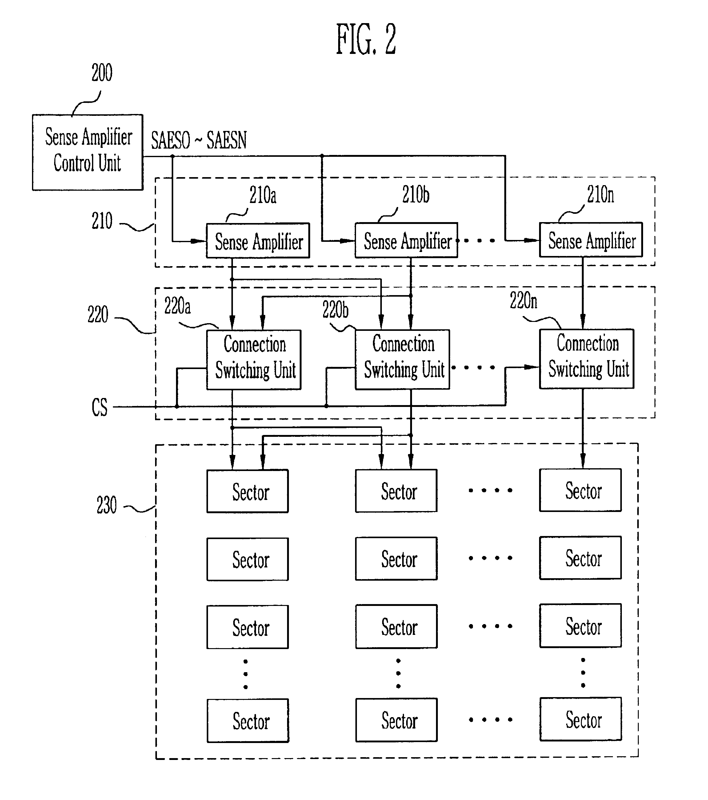
[0027]FIG. 2 is a block diagram of a flash memory device according to a preferred embodiment of the present invention;

[0028]FIG. 3 is a detailed circuit diagram of the sense amplifier shown in FIG. 2; and

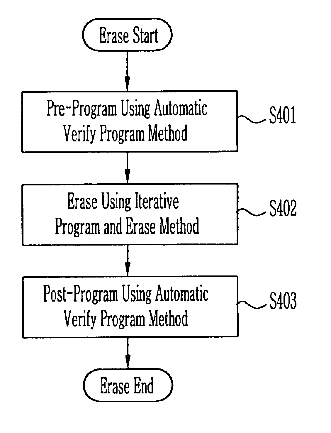
[0029]FIG. 4 is a flowchart for explaining a method of erasing the flash memory device according to a preferred embodiment of the present invention.

DETAILED DESCRIPTION OF PREFERRED EMBODIMENTS

[0030]The present invention will be described in detail by way of a preferred embodiment with reference to accompanying drawings, in which like reference numerals are used to identify the same or similar parts.

[0031]FIG. 2 is a block diagram of a flash memory device according to a preferred embodiment of the present invention.

[0032]Referring now to FIG. 2, the flash memory de...


PUM


Abstract

The present invention relates to a flash memory device and a method of erasing the same. Pre-program and post-program operations are performed using an automatic verify program method, and an erase operation is performed using an iterative program and verify method, by the use of sense amplifiers that can perform the iterative program and verify method and the automatic verify program method.

Description

BACKGROUND OF THE INVENTION[0002]1. Field of the Invention[0003]The invention relates generally to a flash memory device and a method of erasing the same, and more particularly to, a flash memory device and a method of erasing the same, which can improve the erase speed and characteristic of the flash memory device.[0004]2. Description of the Prior Art[0005]In semiconductor nonvolatile memory devices such as EEPROM (electrically erasable and programmable read only memory) and flash memory devices, NOR type semiconductor nonvolatile memory devices (hereinafter called ‘flash memory device’) in which a program operation wherein electrons are injected into a floating gate by means of a channel hot carrier electron (hereinafter called ‘CHE’) injection method is performed and an erase operation using a Fowler-Nordheim (hereinafter called ‘F-N’) tunneling phenomenon is performed, have been widely used.[0006]Generally, the entire data program procedure in this flash memory device includes p...

Claims


Application Information

Patent Timeline
IPC IPC(8): G11C16/34G11C16/28G11C16/06G11C16/12
CPCG11C16/28G11C16/3445G11C16/344G11C16/3409G11C16/3404G11C16/12
Inventor CHANG, SEUNG HO
Owner SK HYNIX INC
Why Eureka
Try Eureka