
Active pixel sensor (APS) readout structure with amplification

a technology readout structure, which is applied in the field of active pixel sensor (aps) imaging devices, can solve the problems of limiting the dynamic range of the sensor, consuming a considerable amount of the chip area, and sacrificing the signal gain of the aps sensor

Inactive Publication Date: 2005-01-18
APTINA IMAGING CORP
View PDF4 Cites 29 Cited by
  • Summary
  • Abstract
  • Description
  • Claims
  • Application Information

AI Technical Summary

Benefits of technology

"The patent describes an active pixel sensor (APS) that includes an array of individually addressable cells. Each cell has a row select transistor and an output transistor, and an amplifier structure that includes a row select transistor and output transistor. The amplifier has a two branched structure, and a transistor may be connected between the output transistor and the p-type transistor in each pixel to protect the output transistor. The amplifier may also have a gain selector to change the gain. The technical effects of this invention include improved sensitivity, reduced noise, and improved linearity of the sensor."

Problems solved by technology

The gain stage of the APS sensor may consume a considerable amount of the chip area.
However, reducing the size of this area may sacrifice signal gain in the APS sensor.
Use of such a transistor may itself limit the dynamic range of the sensor when reading out the pixel and provide a voltage gain less than unity.

Method used


Image

  • Active pixel sensor (APS) readout structure with amplification
  • Active pixel sensor (APS) readout structure with amplification
  • Active pixel sensor (APS) readout structure with amplification

Examples


Embodiment Construction

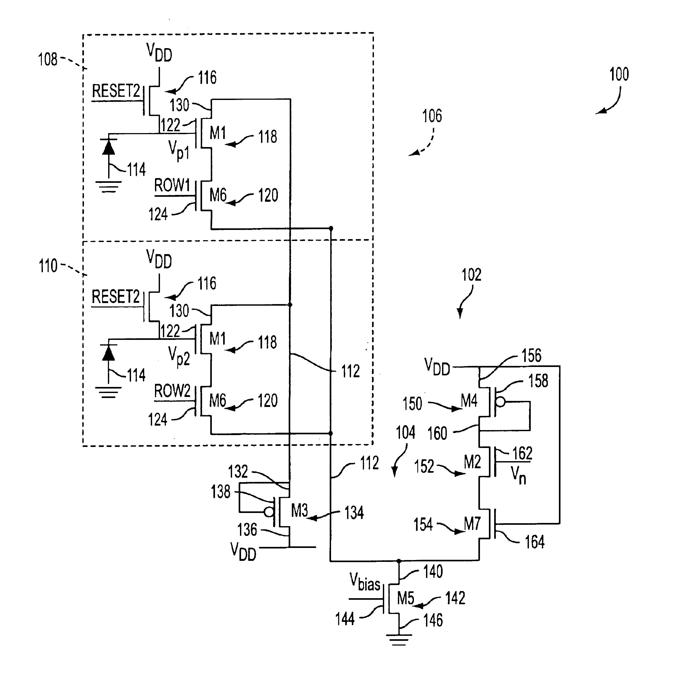
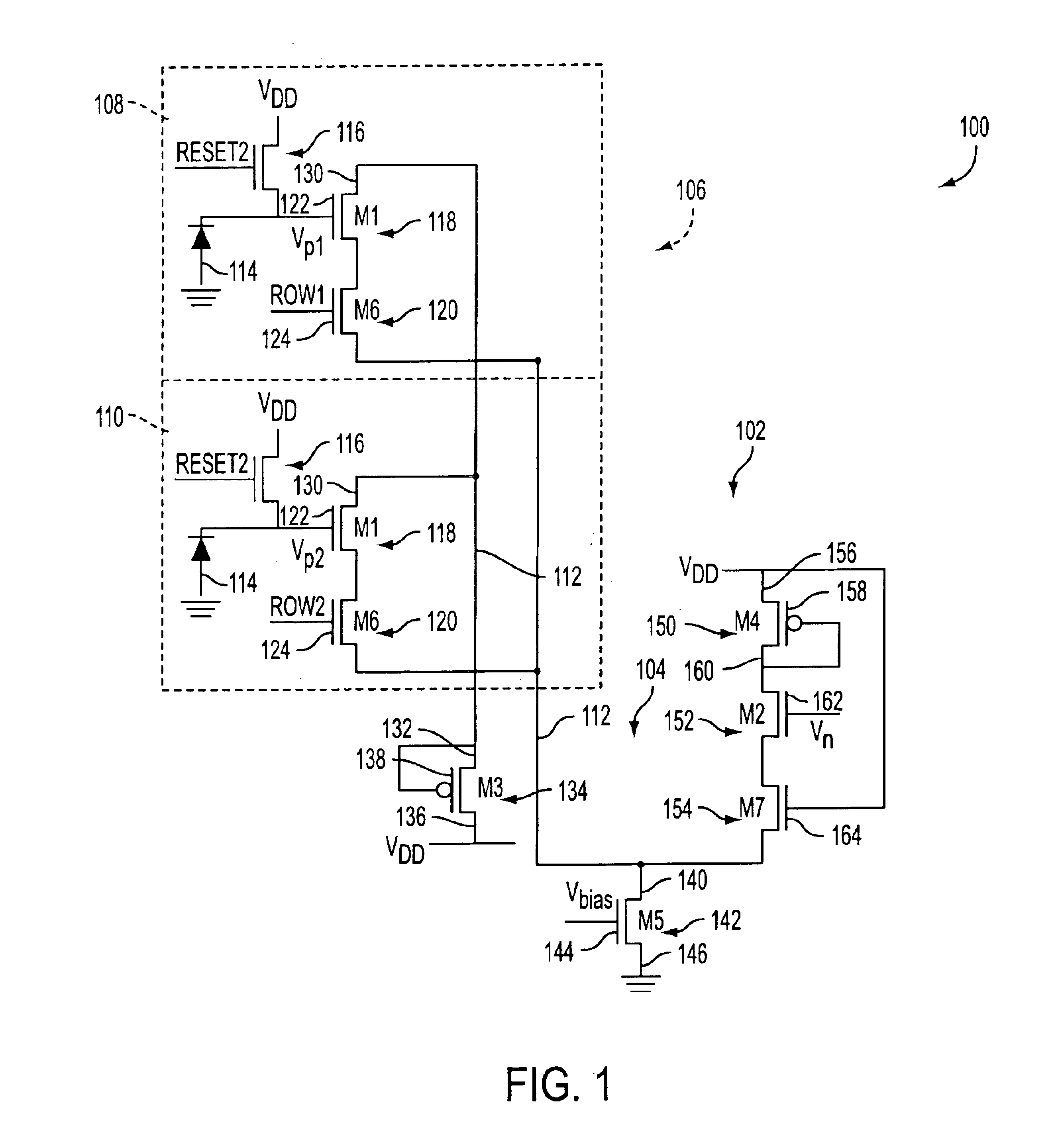
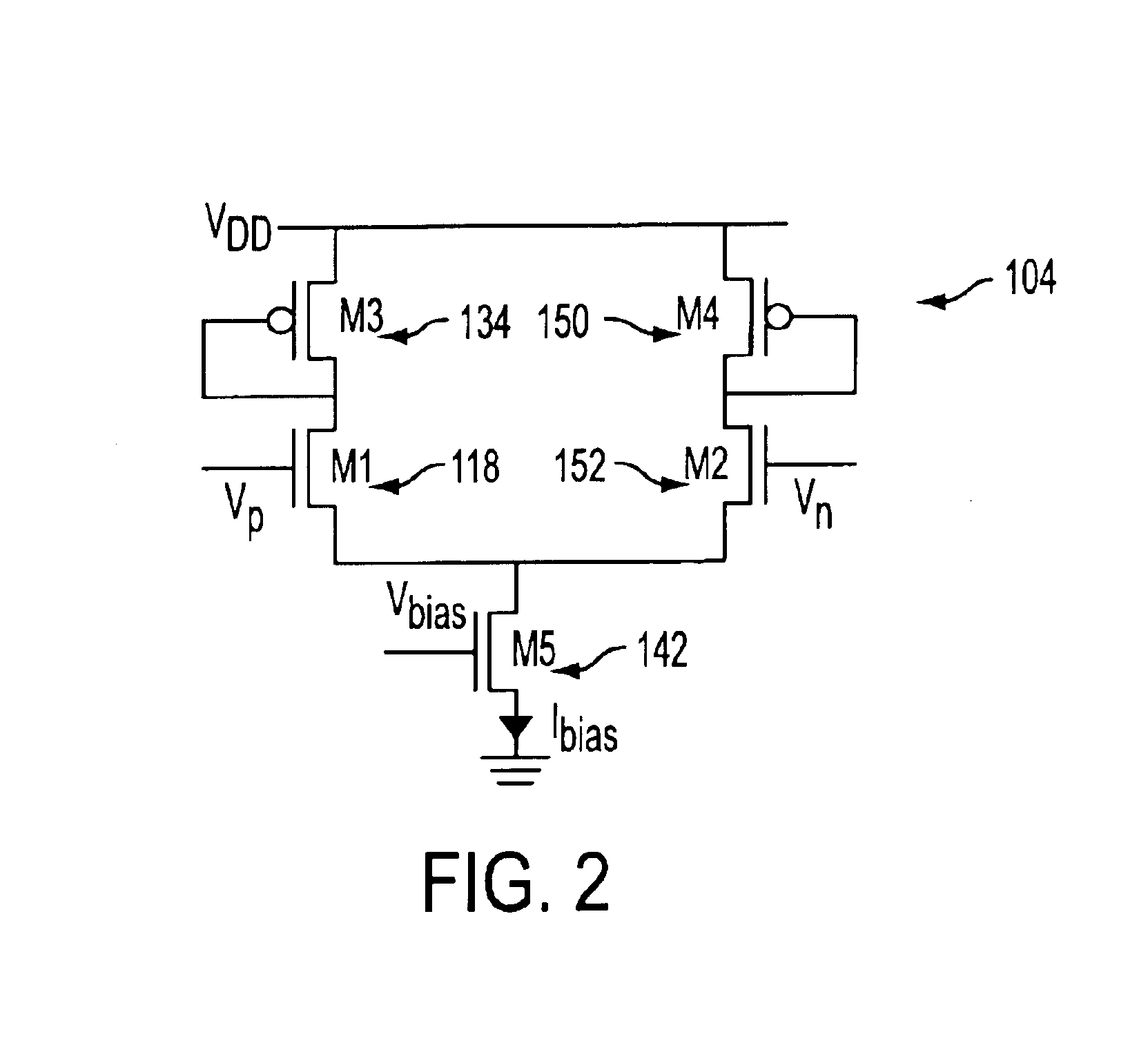
An embodiment is shown in FIG. 1. The readout structure 102 of an active pixel sensor (APS) 100 includes an amplifier circuit 104. The APS includes an array 106 of independently addressable pixels arranged in n rows and m columns. FIG. 1 illustrates two of the pixels 108, 110 that are connected to a column of line 112 of the pixel array. Pixel 108 is in row 1 and pixel 110 is in row 2. Each pixel includes a photodetector 114, such as a photogate, photodiode or pinned photodiode, a reset transistor 116, a source-follower output transistor 118 (denoted M1), and a row select transistor 120 (denoted M6). The gate 122 of the output transistor is connected to a pixel voltage provided by the photodetector. The gate 124 of the row select transistor 120 is connected to a row enable voltage which is set HIGH when the pixel is being read out, thereby allowing the voltage on the output transistor to be passed to the column line 112. The output transistor 118 and row select transistors 120 may b...


PUM


Abstract

An active pixel sensor (APS) includes an array of individually addressable APS cells ad a pixel readout structure that includes an amplifier. The amplifier may have a two-branched structure and provide a gain of one or higher. Additional switches may be provided in the pixels to provide protection for pixel output transistors from voltage changes in the column line. Structure may also be provided for optional gain selection in the amplifier.

Description

BACKGROUNDActive pixel sensor (APS) imaging devices are described in U.S. Pat. No. 5,471,515. These imaging devices include an array of pixel cells that convert light energy into electrical signals. Each pixel includes a photodetector and one or more active transistors formed of MOS technology. The transistors typically provide amplification, readout control and reset control, in addition to producing the electrical signal output from the cell.APS devices may be fabricating using CMOS technology. An APS sensor, including a pixel array and readout structure, may be provided on the same integrated circuit (IC) chip. The gain stage of the APS sensor may consume a considerable amount of the chip area. However, reducing the size of this area may sacrifice signal gain in the APS sensor.The readout structure of an APS typically includes a source follower transistor. Use of such a transistor may itself limit the dynamic range of the sensor when reading out the pixel and provide a voltage ga...

Claims


Application Information

Patent Timeline
Patent Type & Authority Patents(United States)
IPC IPC(8): H04N3/14H04N5/335H04N5/355H04N5/357H04N5/374H04N5/378
CPCH04N5/374H04N5/357H04N25/60H04N25/76H04N25/77
Inventor ANDERSSON, ANDERS
Owner APTINA IMAGING CORP
Learn More