Methods and devices for coupling optoelectronic packages

a technology of optoelectronic packages and coupling devices, applied in the field of methods and devices for coupling optoelectronic packages, can solve the problems of significant reduction of signal power, insufficient alignment, severe consequences, etc., and achieve the effects of preventing the flow of adhesives, improving the coupling of arrays and base chips, and improving the optical coupling of surface devices to fibers

Inactive Publication Date: 2005-02-01
SAMSUNG ELECTRONICS CO LTD
View PDF30 Cites 29 Cited by
  • Summary
  • Abstract
  • Description
  • Claims
  • Application Information

AI Technical Summary

Benefits of technology

In order to provide ease of alignment and coupling of the array to the chip to form the package, only a rear portion of an optical fiber is bonded to the array during assembly of the package. The front portion is left unbonded until after assembly. This allows the front portion of the fiber to remain flexible so that it can be properly positioned relative to the surface device of the base chip.
To prevent the adhesive used in bonding the rear portion from flowing onto the front portion, the arrays envisioned by t

Problems solved by technology

If optical components become disconnected or are improperly aligned (i.e., connected) from the beginning, the consequences can be severe.
Even small misalignments can result in signi

Method used


Image

  • Methods and devices for coupling optoelectronic packages
  • Methods and devices for coupling optoelectronic packages
  • Methods and devices for coupling optoelectronic packages

Examples


Embodiment Construction

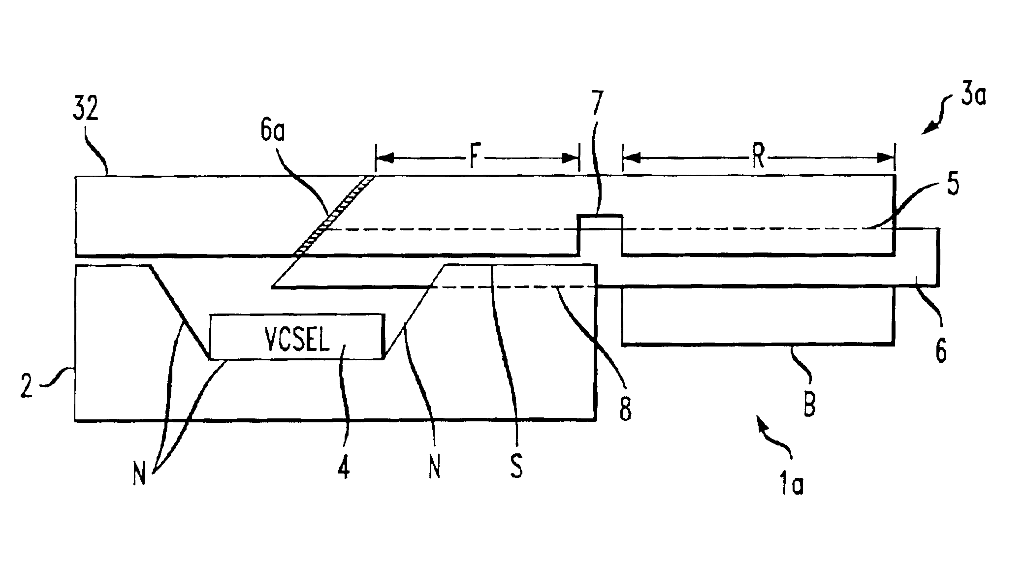
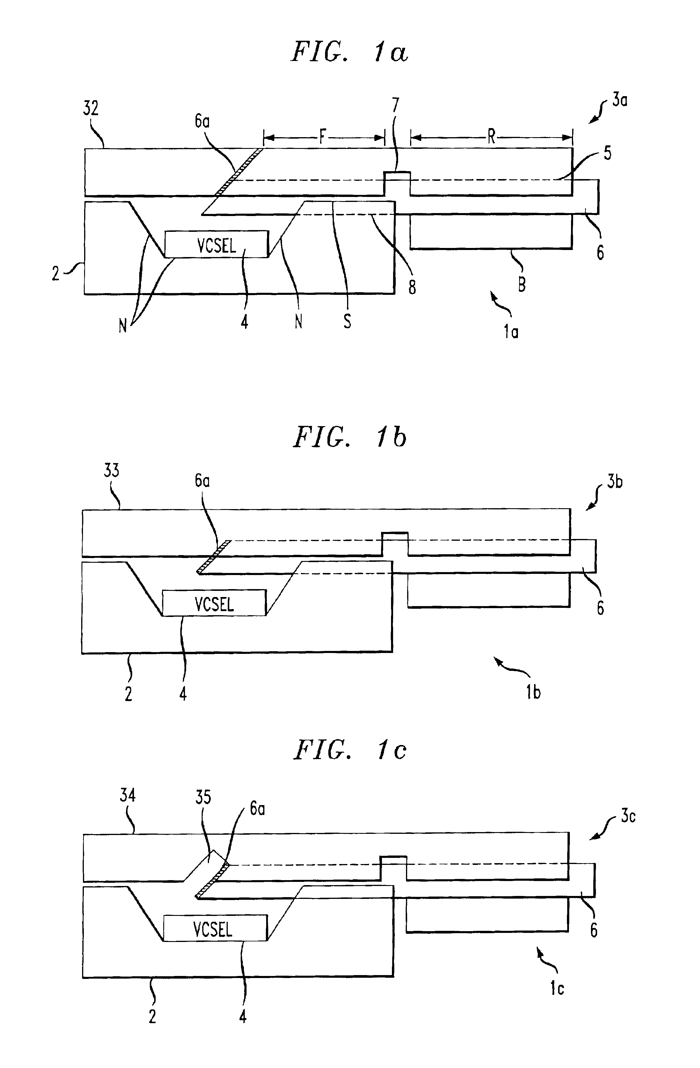
Referring to FIG. 1a there is shown an optoelectronic package 1a according to one embodiment of the present invention. The package 1a comprises a base chip 2 and array 3a. In more detail, the base chip 2 comprises a surface device 4, such as a VCSEL, disposed on a nonmating surface “N” of the chip 2.

In the embodiment shown in FIG. 1a, the array 3a comprises front end sealing lid 32. The sealing lid 32 functions to substantially enclose or shield the VCSEL 4 from the outside environment. There are many ways to affix the sealing lid 32 to the base chip 2. For example, the sealing lid 32 may be soldered to the base chip 2. It should be noted that the lid 32 is separate from the front end portion “F” of array 3a. As such, array 3a can be referred to as a “two-piece” array.

FIGS. 1b and 1c depict two alternative sealing lids 33, 34. In contrast to lid 32, lids 33 and 34 are made from the same substance as the balance of arrays 3b, 3c. Lids 33, 34 and arrays 3b, 3c can be referred to as “m...


PUM


Abstract

Optoelectronic packages comprise both an optical array and base chip. The array and base chip are aligned and coupled using a combination of V-grooves, wick stops, and alignment spheres (e.g., presion ball bearings). The array and base chip are passively aligned by disposeing an optical fiber having an angled endface onto V-grooves in both the array and base chip. The base chip typically comprises an optical surface device, such as a vertical cavity, surface emitting laser or photodetector.

Description

BACKGROUND OF THE INVENTIONNowadays, more and more information is being transmitted over optical fiber or via optical components instead of traditional copper wire. Connecting two components together has always been important. As the trend towards the use of optical components increases, so will the need to insure that such components are correctly connected together. If optical components become disconnected or are improperly aligned (i.e., connected) from the beginning, the consequences can be severe. Even small misalignments can result in significant reductions in signal power.For example, sometimes two separate sets of optical fibers need to be connected together. To do so requires that each set of fibers be properly aligned with one another. There exists a number of methods and devices for connecting both sets of fibers together. These existing methods and devices have drawbacks in that they do not provide for satisfactory alignment or require a relatively long time to do so. N...

Claims


Application Information

Patent Timeline
IPC IPC(8): G02B6/36G02B6/42
CPCG02B6/4239G02B6/4231G02B6/423G02B6/4214
Inventor STEINBERG, DAN A.
Owner SAMSUNG ELECTRONICS CO LTD
Why Eureka
Try Eureka