Optical tap module
a technology of optical tap module and tap module, which is applied in the direction of optics, optical light guides, instruments, etc., can solve the problems of insufficient directivity in the configuration according to the configuration, stray light, and light irradiated onto the chip is reflected by the light shielding film, so as to improve the directivity of the tap module, reduce the reflection of feedback light, and facilitate alignment and assembly
- Summary
- Abstract
- Description
- Claims
- Application Information
AI Technical Summary
Benefits of technology
Problems solved by technology
Method used
Image
Examples
first example
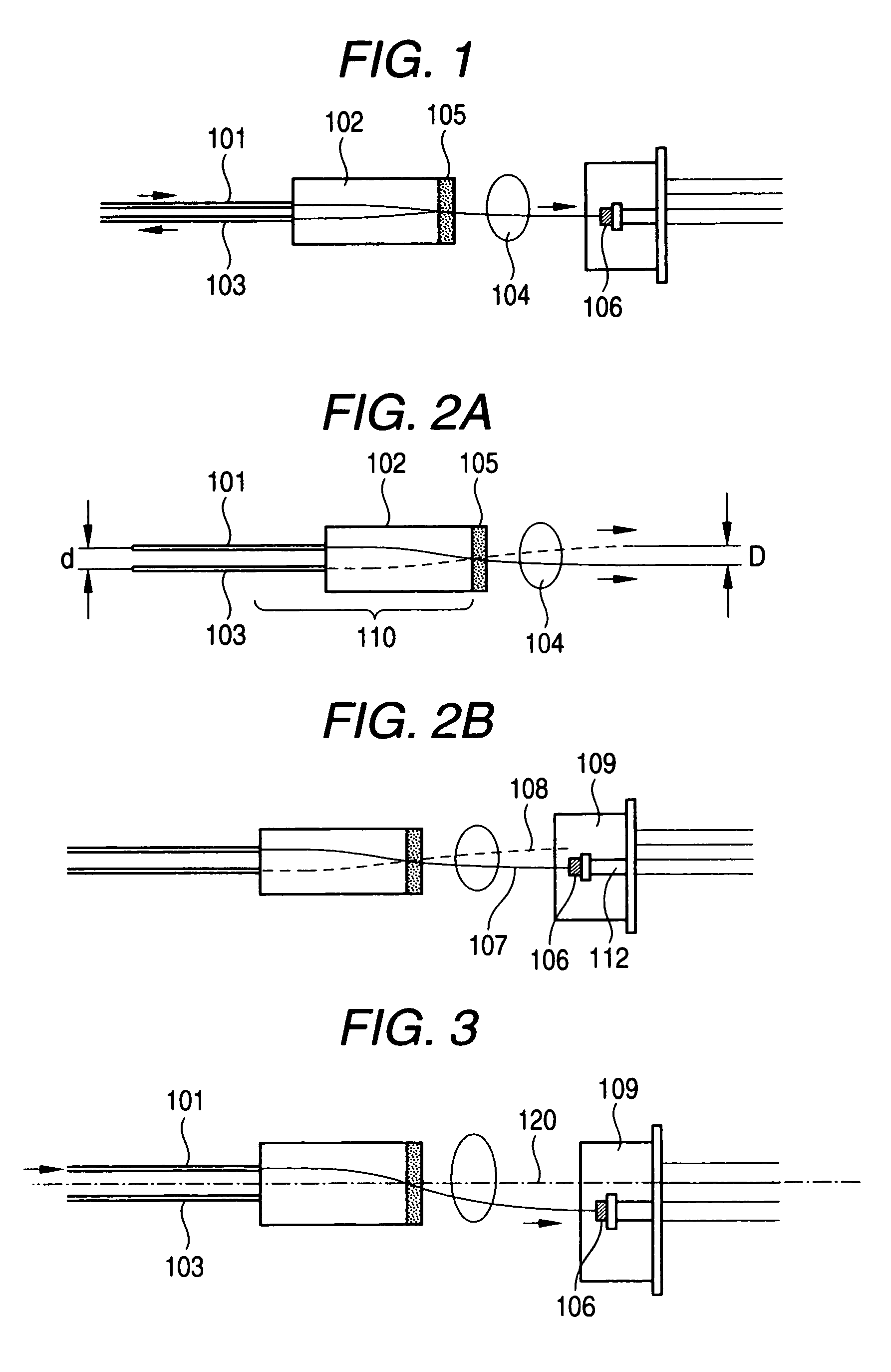
[0088]FIG. 9 shows a unidirectional tap module according to a first example of the invention. Light emitted from an optical fiber 1 for incident light is incident on a gradient index rod lens 2. The gradient index rod lens 2 is manufactured to have 0.25 pitch (meandering cycle) with respect to a used wavelength band, and is designed such that incident light from the optical fiber is emitted as parallel light. Parallel light emitted from the rod lens 2 is incident on an optical filter (tap filter) which is directly formed on an end surface of the rod lens as a thin-layered optical functional element. The filter 5 is designed to have reflectance of 95% and transmittance of 5%.
[0089]Light reflected by the filter 5 is converged by the rod lens 2 again and is incident on an output optical fiber 3. On the other hand, transmitted light from the filter 5 is converged by a second gradient index rod lens (focusing lens) 4 of 0.12 pitch, and is incident on a photodiode 6. Further, the emitting...
second example
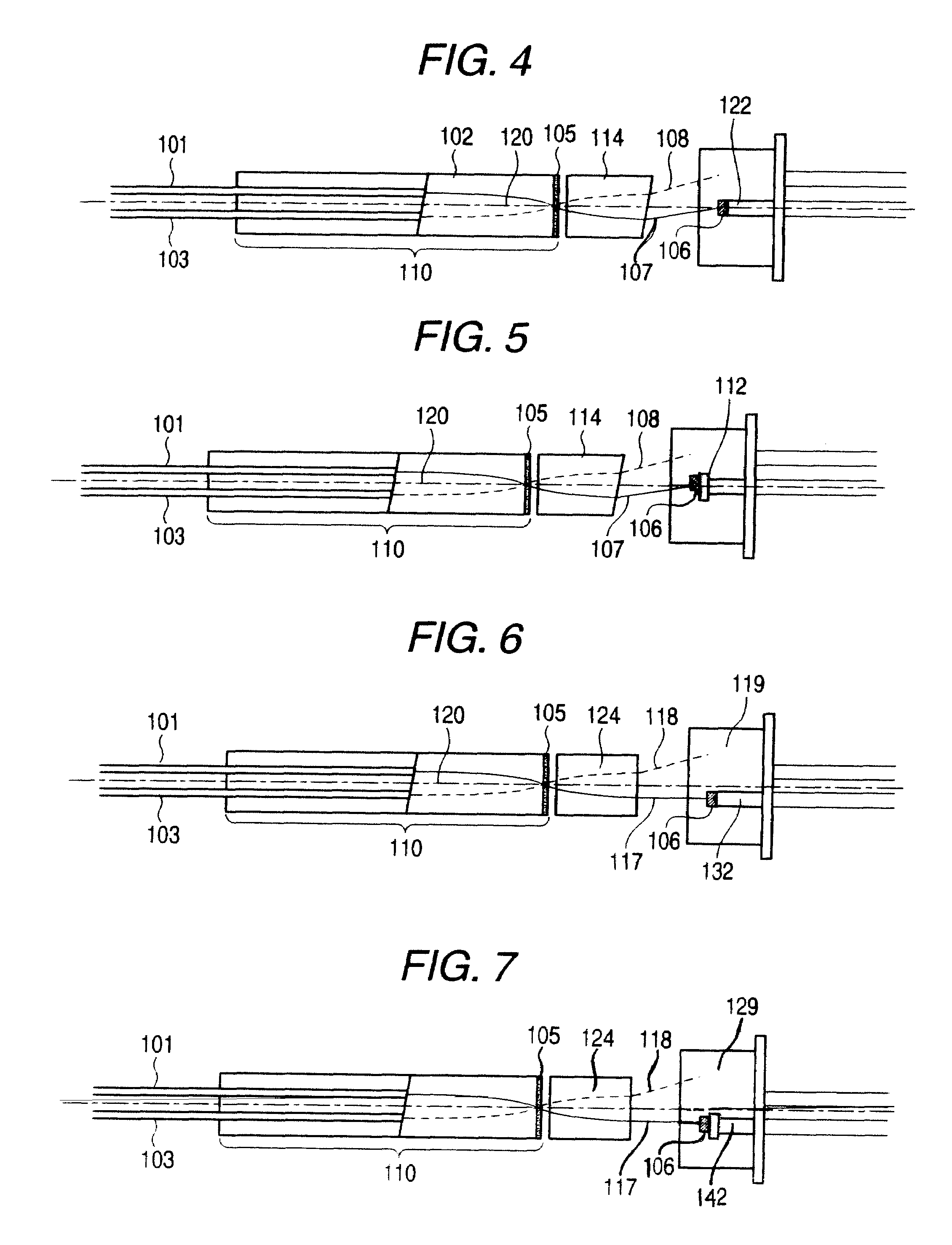
[0095]FIG. 11 shows of a unidirectional tap module according to a second example of the invention. The optical fibers 1 and 3, the two-core capillary 7 supporting the optical fibers 1 and 3, the rod lenses 2 and 4 are the same as those in the first example. However, the tap filter 15 was designed to have reflectance of 99% and transmittance of 1%. As a pin 22, on which the chip of a package 19 was mounted, a straight pin, not a normal nail pin, was used. The diameter of the pin 22 was 0.45 mm. The chip of the photodiode 6 had the diagonal size of 240 μm, like the first example.
[0096]The chip was mounted on the end surface of the pin 22. In this example, as shown in FIG. 11, the entire package 9 of the photodiode was obliquely fixed by 8° so as to reduce reflection feedback light. If the surface of the pin is processed obliquely, and the chip is mounted, the package does not need to be inclined.
[0097]When the directivity of the module was measured, the same result as the first exampl...
PUM
 Abstract
Description
Claims
Application Information


