

Light emitting device and method of fabricating the same
a technology of light emitting devices and light leakage regions, which is applied in the manufacture of semiconductor/solid-state devices, semiconductor devices, electrical devices, etc., can solve the problems of reducing the substantial light extraction energy from the light leakage region, increasing the electrode area, and increasing the amount of light extraction energy, so as to increase the flux extractable, increase the current spreading effect, and make the current spreading effect more distinctiv
- Summary
- Abstract
- Description
- Claims
- Application Information
AI Technical Summary
Benefits of technology
Problems solved by technology
Method used
Image

Examples
Embodiment Construction
[0034] Best modes for carrying out this invention will be described below referring to the attached drawings.
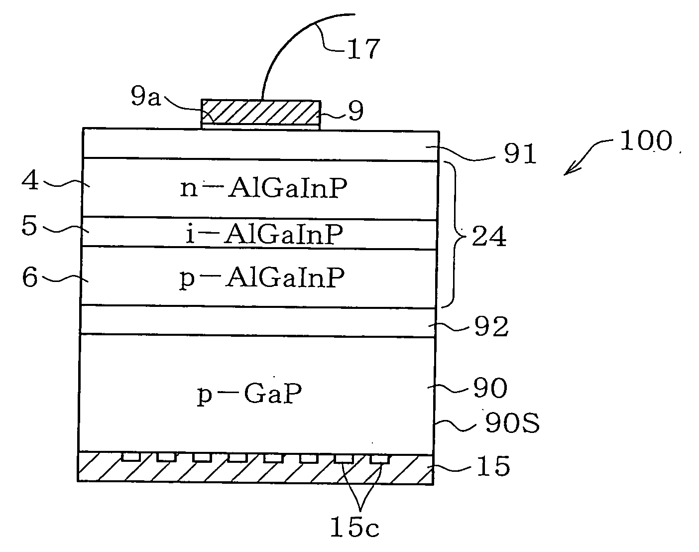
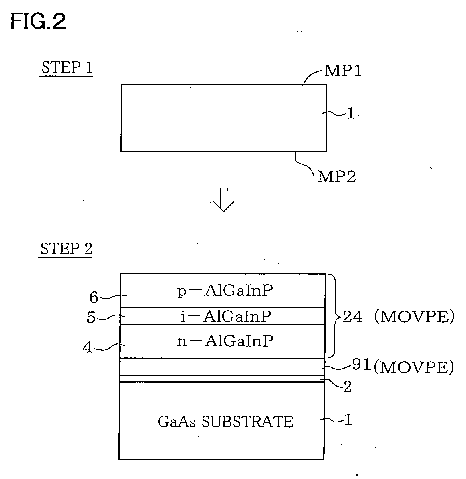
[0035]FIG. 1 is a conceptual drawing of a light emitting device 100 as one embodiment of this invention. The light emitting device 100 has a light emitting layer portion 24 composed of a III-V compound semiconductor; and a transparent thick-film semiconductor layer 90 formed on the second main surface side of the light emitting layer portion 24, and composed of a III-V compound semiconductor having a band gap energy larger than a light quantum energy which corresponds to a peak wavelength of emission flux from the light emitting layer portion 24.
[0036] The light emitting layer portion 24 has a structure in which an active layer 5 composed of a non-doped (AlxGa1-x)yIn1-yP alloy (where, 0≦x≦0.55, 0.45≦y≦0.55) is held between a p-type cladding layer 6 composed of a p-type (AlzGa1-z)yIn1-yP alloy (where, x4 composed of an n-type (AlzGa1-z)yIn1-yP alloy (where, x100 shown in FIG...
PUM
 Abstract
Description
Claims
Application Information