

Epitaxial growth method with p-layer special doped structure
An epitaxial growth, special technology, applied in the direction of electrical components, semiconductor/solid-state device manufacturing, circuits, etc., can solve the problem of difficult to generate high carrier concentration, growth conditions, reduce material quality and other problems, to reduce the self-compensation effect , Improve crystal quality, improve the effect of doping effect
- Summary
- Abstract
- Description
- Claims
- Application Information
AI Technical Summary
Problems solved by technology
Method used
Image

Examples
Embodiment Construction
[0044] The present invention will be further elaborated below in conjunction with the accompanying drawings.
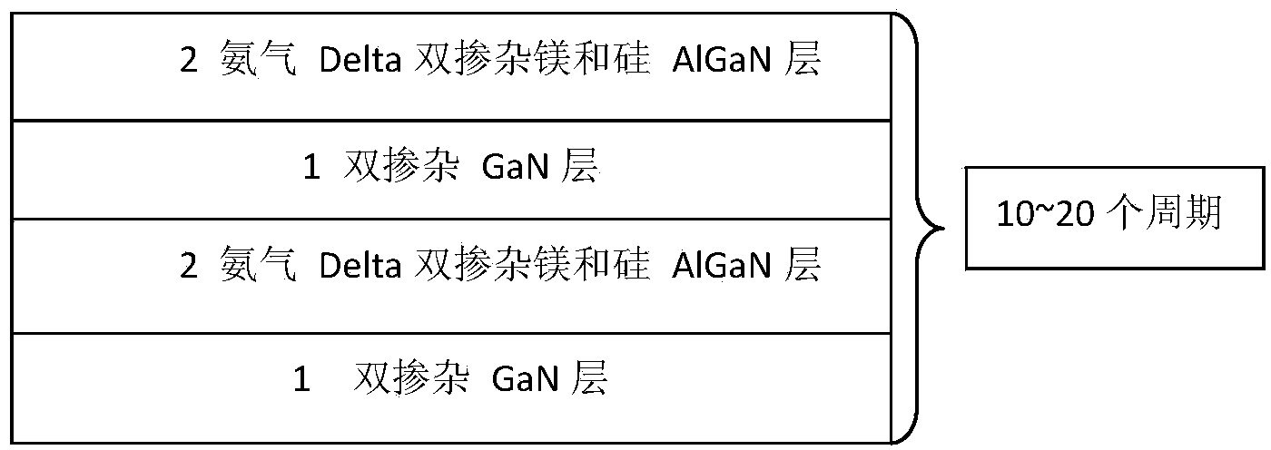
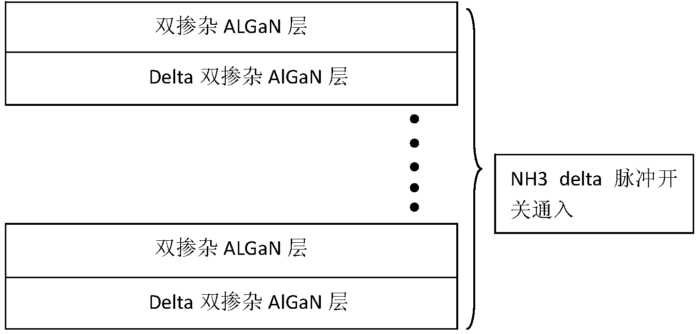
[0045] The present invention applies metal organic compound chemical vapor deposition (MOCVD) epitaxial growth technology, utilizes existing MOCVD technology equipment, uses trimethylgallium (TMGa), triethylgallium (TEGa), and trimethylindium (TMIn), Trimethylaluminum (TMAl) and ammonia (NH3) silane (SiH4) and dimagnesium (cp2Mg) respectively provide gallium source, indium source, aluminum source, and nitrogen source, magnesium source, silicon source required for growth, using NH3 pulsed delta doping is used to prepare p-layer superlattice structure with double element doping, which further combines the advantages of delta doping and double doping.
[0046] A specific example of the epitaxial growth method is as follows:
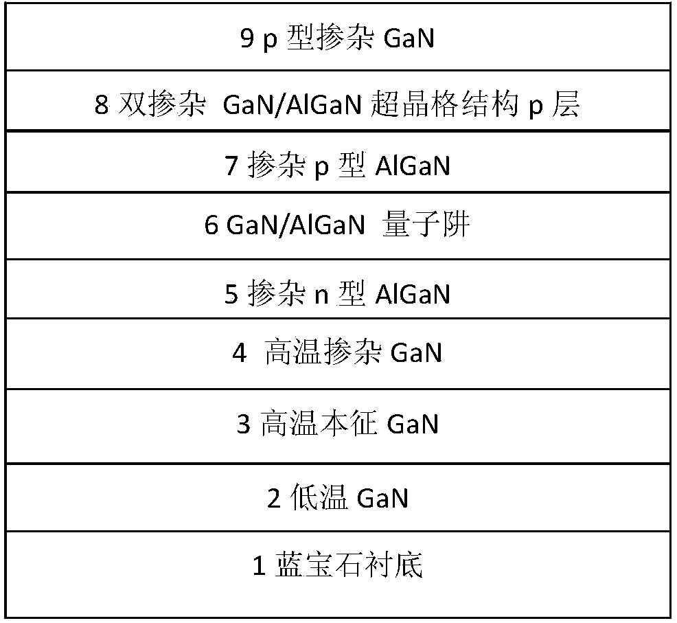
[0047] 1. After the sapphire substrate is specially cleaned, put it into the MOCVD equipment and bake it at 1100°C for 10 minutes.
[0048] 2. Lo...
PUM
 Abstract
Description
Claims
Application Information