LED epitaxial wafer, manufacturing method thereof and semiconductor device

A technology of LED epitaxial wafers and manufacturing methods, which is applied in the direction of semiconductor devices, electrical components, circuits, etc., can solve the problems of small-sized chips such as increased current density, hindered hole transmission, and sudden drop in efficiency, so as to reduce the polarization electric field , Improve luminous efficiency and reduce the effect of sudden drop in efficiency

Pending Publication Date: 2019-11-22
XIAMEN CHANGELIGHT CO LTD
View PDF0 Cites 5 Cited by
  • Summary
  • Abstract
  • Description
  • Claims
  • Application Information

AI Technical Summary

Problems solved by technology

However, with the current development of Micro / Min LED, the continuous reduction of chip size will inevitably bring about other problems, such as the increase of current density and serious electron leakage caused by the small size chip under the same current injection. At the same time, due to the use of P The type electron blocking layer also hinders the further transport of holes, resulting in a sharp drop in efficiency

Method used


Image

  • LED epitaxial wafer, manufacturing method thereof and semiconductor device
  • LED epitaxial wafer, manufacturing method thereof and semiconductor device
  • LED epitaxial wafer, manufacturing method thereof and semiconductor device

Examples


Embodiment Construction

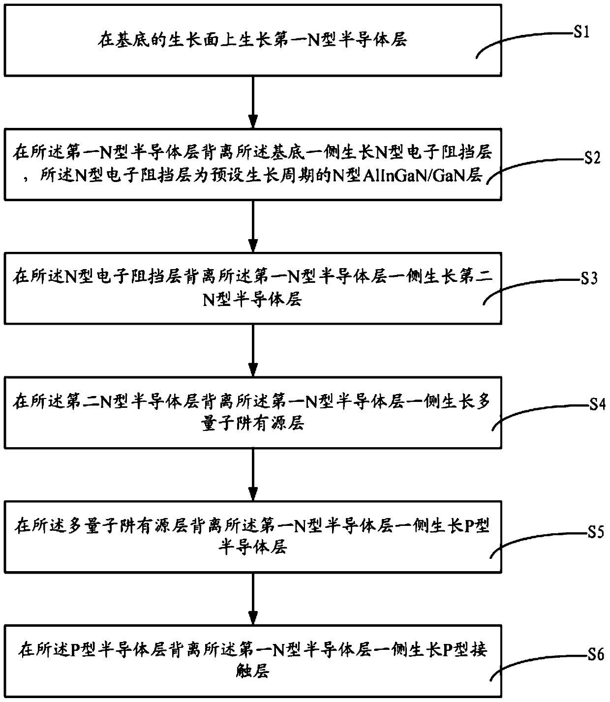
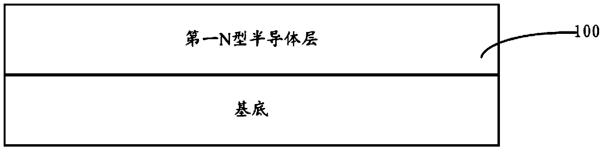
[0041] The following will clearly and completely describe the technical solutions in the embodiments of the present invention with reference to the accompanying drawings in the embodiments of the present invention. Obviously, the described embodiments are only some, not all, embodiments of the present invention. Based on the embodiments of the present invention, all other embodiments obtained by persons of ordinary skill in the art without making creative efforts belong to the protection scope of the present invention.

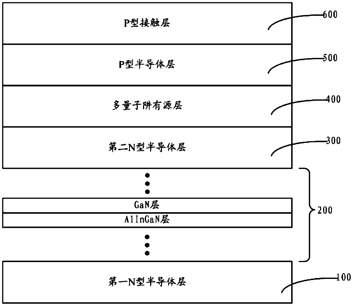
[0042] As mentioned in the background technology, in recent years, III-V nitrides have been widely used in the fields of electronics and optics due to their excellent physical and chemical properties (large band gap, high breakdown electric field, high electron saturation mobility, etc.) . Among them, the blue-green light-emitting diode with GaN base as the main material has made great progress in lighting, display and digital. However, with the current devel...


PUM


Abstract

The invention discloses an LED epitaxial wafer, a manufacturing method thereof and a semiconductor device. An N-type electron barrier layer is embedded between a first N-type semiconductor layer and asecond N-type semiconductor layer. The N-type electron barrier layer is an N-type AlInGaN / GaN layer; as the lattice mismatch of AlInGaN and GaN in the N-type AlInGaN / GaN layer is relatively small, through stress modulation, a polarization electric field of a quantum well region is reduced, so that adverse effects caused by sudden efficiency drop can be reduced, and meanwhile, the lateral currentexpansion capability of the LED epitaxial wafer is also improved, so that the semiconductor device has good current expansion capability. Moreover, the P-type electron barrier layer is removed from the LED epitaxial wafer, so that hole injection can be increased, uneven distribution of carriers in the quantum wells is relieved, the multi-quantum-well active layer emits light more uniformly, the light emitting efficiency of the LED epitaxial wafer is improved, and the performance of the semiconductor device is improved.

Description

technical field [0001] The present invention relates to the technical field of semiconductor light emitting, and more specifically, relates to an LED (Light Emitting Diode, light emitting diode) epitaxial wafer, a manufacturing method thereof, and a semiconductor device. Background technique [0002] In recent years, III-V nitrides have been widely used in the fields of electronics and optics due to their excellent physical and chemical properties (large band gap, high breakdown electric field, high electron saturation mobility, etc.). Among them, the blue-green light-emitting diode with GaN base as the main material has made great progress in lighting, display and digital. However, with the current development of Micro / Min LED, the shrinking chip size will inevitably bring about other problems, such as the increase of current density and serious electron leakage caused by small-sized chips under the same current injection. At the same time, due to the use of P The type ele...

Claims


Application Information

Patent Timeline
Patent Type & Authority Applications(China)
IPC IPC(8): H01L33/14H01L33/06H01L33/32H01L33/00
CPCH01L33/0075H01L33/06H01L33/145H01L33/32
Inventor 万志卓祥景尧刚程伟林志伟
Owner XIAMEN CHANGELIGHT CO LTD
Why Eureka
Try Eureka