Epitaxial wafer of light-emitting diode and its preparation method

A technology of light-emitting diodes and epitaxial wafers, applied in semiconductor devices, electrical components, circuits, etc., can solve the problems of low luminous efficiency of MiniLED, tilted quantum well band, and reduced radiation recombination efficiency, so as to improve the carrier localization effect. , the effect of improving the energy band tilt and weakening the polarization electric field

Active Publication Date: 2022-03-18
HC SEMITEK ZHEJIANG CO LTD
View PDF5 Cites 0 Cited by
  • Summary
  • Abstract
  • Description
  • Claims
  • Application Information

AI Technical Summary

Problems solved by technology

[0004] In related technologies, in the growth of Mini LED epitaxy technology, InGaN / GaN materials are used to make multiple quantum wells. Since the lattice constant of InGaN materials is larger than that of GaN, they are subjected to compressive stress, and the compressive stress increases with the increase of In composition. Severe lattice mismatch will directly affect the intensity of piezoelectric polarization. The polarization electric field will cause the energy band of the quantum well to tilt, making the overlap of the electron-hole wave function smaller, and the defects and dislocations in the bottom layer will extend to the quantum well region. A large number of defects and dislocations will reduce the radiation recombination efficiency, resulting in low luminous efficiency of Mini LED

Method used


Image

  • Epitaxial wafer of light-emitting diode and its preparation method
  • Epitaxial wafer of light-emitting diode and its preparation method
  • Epitaxial wafer of light-emitting diode and its preparation method

Examples


Embodiment Construction

[0026] In order to make the purpose, technical solution and advantages of the present disclosure clearer, the implementation manners of the present disclosure will be further described in detail below in conjunction with the accompanying drawings.

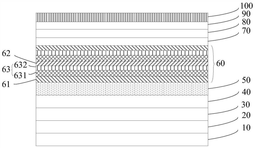
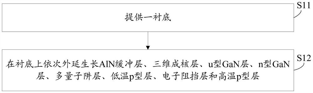
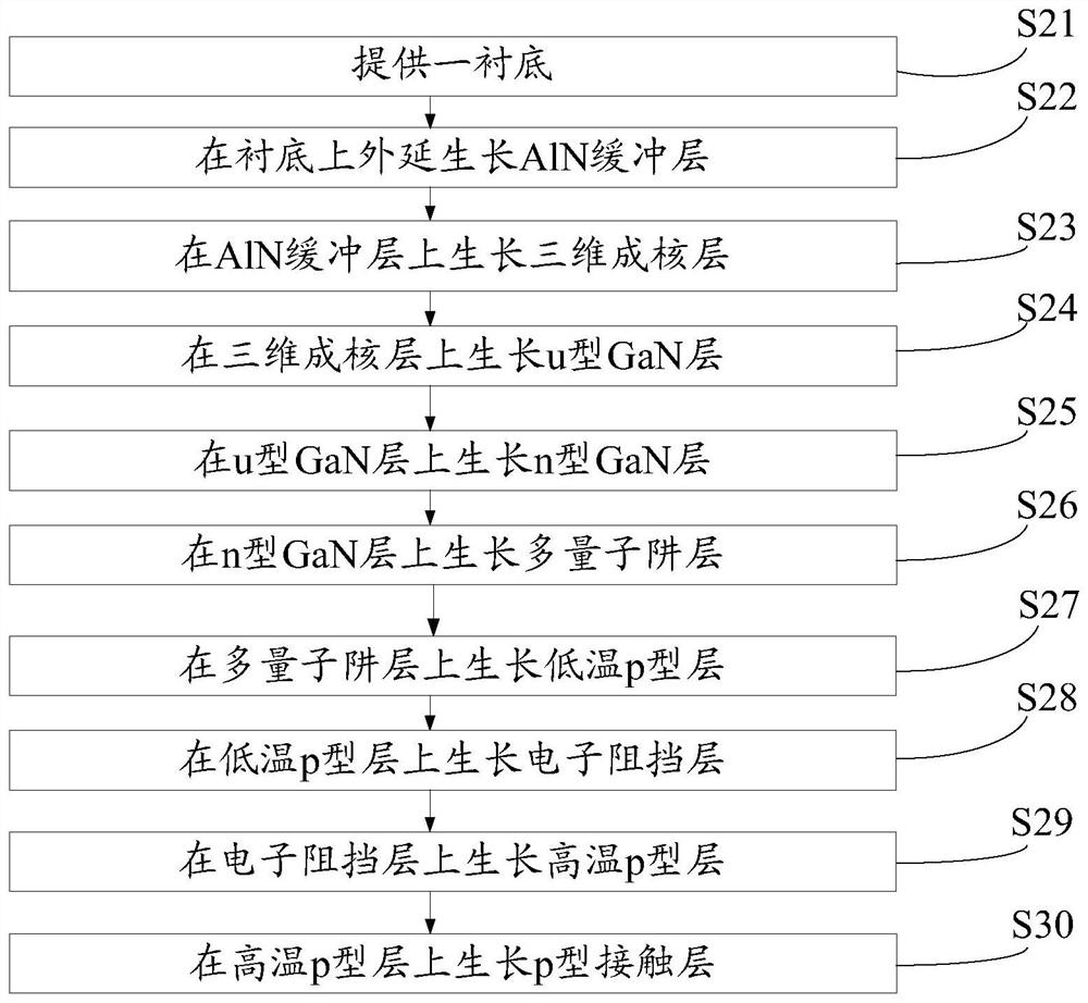
[0027] figure 1 It is a schematic structural diagram of an epitaxial wafer of a light emitting diode provided by an embodiment of the present disclosure. Such as figure 1 As shown, the epitaxial wafer includes a substrate 10 and an AlN buffer layer 20, a three-dimensional nucleation layer 30, a u-type GaN layer 40, an n-type GaN layer 50, a multi-quantum well layer 60, and a low-temperature p type layer 70, electron blocking layer 80 and high temperature p-type layer 90.

[0028] Wherein, the multi-quantum well layer 60 includes a plurality of In x Ga 1-x N quantum well layer 61 and a plurality of GaN quantum barrier layers 62, and the In x Ga 1-x A composite structure 63 between the N quantum well layer 61 and the GaN quantu...


PUM

PropertyMeasurementUnit
thicknessaaaaaaaaaa
thicknessaaaaaaaaaa
temperatureaaaaaaaaaa

Abstract

The disclosure provides an epitaxial wafer of a light emitting diode and a preparation method thereof, which belong to the technical field of optoelectronic manufacturing. The epitaxial wafer includes a substrate, an AlN buffer layer, a three-dimensional nucleation layer, a u-type GaN layer, an n-type GaN layer, a multi-quantum well layer, a low-temperature p-type layer, an electron blocking layer, and a high-temperature p-type layer. The multi-quantum well layer includes Multiple In x Ga 1‑x N quantum well layer and multiple GaN quantum barrier layers, and the In x Ga 1‑x Composite structure between N quantum well layer and GaN quantum barrier layer, the composite structure includes n-In y Ga 1‑y N layer and SiN layer. n‑In y Ga 1‑y The Si atoms in the N layer can fill the defect vacancies in the InGaN material. The InGaN material with a lower In composition is conducive to weakening the polarization electric field and improving the energy band tilt. The SiN layer is conducive to the uniformity of carriers in the multi-quantum well layer. Diffusion, improve the carrier localization effect, and improve the luminous efficiency of LED.

Description

technical field [0001] The disclosure relates to the technical field of optoelectronic manufacturing, in particular to an epitaxial wafer of a light emitting diode and a preparation method thereof. Background technique [0002] LED (Light Emitting Diode, light-emitting diode) has the advantages of small size, long life, low power consumption, etc., and is currently widely used in automobile signal lights, traffic lights, display screens and lighting equipment, especially for the resolution and display quality of display devices. The requirements are getting higher and higher, and the application of Mini LEDs is also increasing. [0003] At present, GaN-based LED epitaxial wafers usually include a substrate and an AlN buffer layer, a three-dimensional nucleation layer, a u-type GaN layer, an n-type GaN layer, a multi-quantum well layer and a p-type layer grown sequentially on the substrate. After the LED is energized, carriers (including electrons in the n-type GaN layer and...

Claims


Application Information

Patent Timeline
Patent Type & Authority Patents(China)
IPC IPC(8): H01L33/06H01L33/12H01L33/14H01L33/00
CPCH01L33/06H01L33/12H01L33/14H01L33/145H01L33/0075H01L33/007
Inventor 洪威威尚玉平梅劲董彬忠
Owner HC SEMITEK ZHEJIANG CO LTD
Why Eureka
Try Eureka