GaN-based semiconductor device with compound graded quantum barrier structure and its manufacturing method

A gallium nitride-based, multi-quantum well structure technology, applied in the field of gallium nitride-based semiconductor devices, gallium nitride-based semiconductor devices and their preparation, can solve the problem of reducing electron-hole recombination efficiency and hindering carrier hole injection etc. to achieve the effects of reducing electron leakage, improving hole transport, and making the preparation process simple and controllable

Active Publication Date: 2018-08-10
杭州增益光电科技有限公司
View PDF5 Cites 0 Cited by
  • Summary
  • Abstract
  • Description
  • Claims
  • Application Information

AI Technical Summary

Problems solved by technology

[0003] see figure 2 The traditional InGaN / GaN multi-quantum well structure energy band diagram shown, in which due to the existence of the polarization electric field along the growth direction, the energy bands of quantum wells and quantum barriers are tilted, which reduces the electron-hole recombination efficiency, and the formed potential barrier Spikes hinder the injection of carriers, especially holes

Method used


Image

  • GaN-based semiconductor device with compound graded quantum barrier structure and its manufacturing method
  • GaN-based semiconductor device with compound graded quantum barrier structure and its manufacturing method
  • GaN-based semiconductor device with compound graded quantum barrier structure and its manufacturing method

Examples


Embodiment Construction

[0020] The technical solution of the present invention will be further explained below in conjunction with the accompanying drawings and preferred embodiments, but the specific implementation of the present invention is not limited thereto.

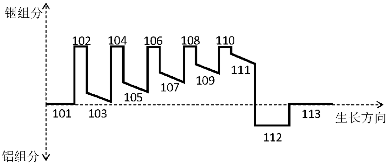
[0021] see figure 1 Shown is a schematic diagram of the indium composition in the multi-quantum well in a GaN-based LED device in a typical embodiment of the present invention and the aluminum composition in the AlGaN electron blocking layer above the multi-quantum well, and its growth direction is from the N-type Pointing to the P-type direction, 102, 104, 106, 108, and 110 are all InGaN quantum wells, and 101, 103, 105, 107, 109, and 111 are InGaN quantum barriers. The first barrier 101 is not graded, and the other barriers are all graded composition, and the indium composition gradually decreases from N to P. On average, the average indium composition in different barriers increases gradually from N to P direction.

[0022] see agai...


PUM

PropertyMeasurementUnit
thicknessaaaaaaaaaa
thicknessaaaaaaaaaa

Abstract

The invention discloses a GaN-based semiconductor device with a composite gradual-change quantum barrier structure and a preparation method of the semiconductor device. The device comprises a multi-quantum well structure, the multi-quantum well structure comprises InGaN layers which grown alternatively, the average In content in the different quantum barrier layers in the multi-quantum well structure is reduced gradually from the P type side to the N type side, and the In content in at least one quantum barrier layer is increased gradually from the P type side to the N type side. Due to use of the composite gradual-change quantum barrier structure in the device, the polarized electric field in the quantum well region can be reduced, the electron-hole composite efficiency is increased, hole transportation is improved, distribution non-uniformity of the holes among wells is reduced, leakage of electrons is reduced, the light emitting efficiency of LED devices and the like can be improved obviously, the problem of decrease of the light emitting efficiency is inhibited substantially, preparation technology is simple and controllable, and convenience is provided for large-scale enforcement.

Description

technical field [0001] The invention relates to a gallium nitride-based semiconductor device, in particular to a gallium nitride-based semiconductor device with a composite gradient quantum barrier structure and a preparation method thereof, belonging to the field of gallium nitride optoelectronic devices. Background technique [0002] Gallium nitride light-emitting diodes are widely used in display, lighting and other fields due to their low power consumption, long life, high efficiency, and environmental protection. However, there is a strong polarization electric field in AlInGaN materials grown in the c-direction, which causes the energy bands of the quantum wells to incline, so that electrons and holes are separated in space, and the recombination luminous efficiency is reduced. Moreover, the potential barrier peak generated by the energy band inclination will block the transport of holes, and the effective mass of the holes is very large, so that the distribution of ho...

Claims


Application Information

Patent Timeline
Patent Type & Authority Patents(China)
IPC IPC(8): H01L33/04H01L31/0352H01L31/18H01L33/00
Inventor 张峰池田昌夫周坤刘建平张书明李德尧张立群杨辉
Owner 杭州增益光电科技有限公司
Why Eureka
Try Eureka