Epitaxial structure of gallium nitride based laser device and manufacturing method of epitaxial structure

A gallium nitride-based, epitaxial structure technology, applied in lasers, laser parts, semiconductor lasers, etc., can solve the problems of reducing laser performance, increasing laser light absorption, etc., to reduce non-radiative recombination and carrier absorption, The effect of reducing the polarization electric field and reducing the accumulation of electrons

Active Publication Date: 2013-10-09
HANGZHOU HONGSHI TECH
View PDF4 Cites 0 Cited by
  • Summary
  • Abstract
  • Description
  • Claims
  • Application Information

AI Technical Summary

Problems solved by technology

However, for the III-V nitride epitaxial structure grown on the (0001)c polar plane, the GaN barrier layer (hereinafter referred to as the uppermost GaN barrier layer) in the traditional quantum well active region is closest to the p-type layer. There will be a sudden change in composition between AlGaN and AlGaN electron blocking layers, which will lead to changes in potential distribution and electronic band structure, resulting in a large built-in polarization electric field and electron accumulation on the interface; and electron accumulation It will cause non-radiative recombination or overflow the active area, and may also increase the light absorption of the laser as an absorption area, these effects will reduce the performance of the laser

Method used


Image

  • Epitaxial structure of gallium nitride based laser device and manufacturing method of epitaxial structure
  • Epitaxial structure of gallium nitride based laser device and manufacturing method of epitaxial structure
  • Epitaxial structure of gallium nitride based laser device and manufacturing method of epitaxial structure

Examples


Embodiment 1

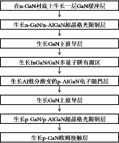
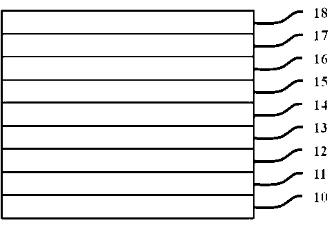
[0033] see Figure 1~3 As shown, a method for preparing a GaN-based laser epitaxial structure includes the following steps:

[0034] (a) epitaxially grow a GaN buffer layer on the n-GaN substrate;

[0035] (b) Epitaxial growth of n-GaN / n-AlGaN superlattice n-type optical confinement layer on the buffer layer;

[0036] (c) Growth of undoped GaN lower waveguide layer;

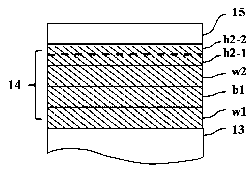
[0037] (d) Growth of InGaN / GaN quantum well active region;

[0038] (e) Growth of Al with graded Al composition x Ga 1-x N electron blocking layer;

[0039] (f) growing an undoped GaN upper waveguide layer;

[0040] (g) Growth of p-GaN / p-AlGaN superlattice p-type optical confinement layer;

[0041] (h) Growth of p-GaN ohmic contact layer.

[0042] After the step (h), it further includes: using inductively coupled plasma (ICP) to etch a laser ridge structure; using electron beam evaporation or magnetron sputtering to deposit a layer of dielectric film on the surface of the top p-GaN contact layer As a lat...


PUM


Abstract

The invention discloses a preparation method of an epitaxial structure of a gallium nitride based laser device, comprising the following steps of: (a) epitaxially growing one GaN buffer layer on a substrate; (b) epitaxially growing an n-type light limiting layer on the buffer layer; (c) growing a lower waveguide layer; (d) epitaxially growing an InaGa1-aN / GaN multi-quantum well as an active region; after growing the last InaGa1-aN / GaN multi-quantum well, replacing the last GaN barrier layer by an AlGaN layer, wherein the AlGaN layer is an AlxGa1-xN which is 1-50 nm in thickness and has gradually-changed Al components or is composed of at least two layers of AlyGa1-yN layers with gradually-increased Al components; (e) epitaxially growing one p-type AlzGa1-zN electron blocking layer, wherein in the steps (d) and (e), x is more than or equal to 0 and is less than or equal to y, y is more than or equal to x and is less than or equal to z, and z is more than or equal to y and is less than or equal to 1; (f) growing an upper waveguide layer; (g) growing a p-type light limiting layer; and (h) growing an ohm contact layer. According to the preparation method provided by the invention, the problem of electron accumulation of the uppermost GaN barrier layer and an AlGaN electron blocking layer is solved, and the performance of the laser device is effectively improved.

Description

technical field [0001] The invention relates to a GaN-based laser epitaxial structure and a preparation method thereof, belonging to the field of laser structure design in semiconductor technology. Background technique [0002] In the prior art, GaN-based lasers (LDs) and light-emitting diodes (LEDs) both use a single layer of Al with a fixed Al component. x Ga 1-x N (usually x~0.2) acts as an electron blocking layer. However, for the III-V nitride epitaxial structure grown on the (0001)c polar plane, the GaN barrier layer (hereinafter referred to as the uppermost GaN barrier layer) in the traditional quantum well active region is closest to the p-type layer. There will be a sudden change in the composition between AlGaN and the AlGaN electron blocking layer. The sudden change in the composition will lead to changes in the potential distribution and electronic band structure, resulting in a large built-in polarization electric field and electron accumulation on the interfa...

Claims


Application Information

Patent Timeline
Patent Type & Authority Patents(China)
IPC IPC(8): H01S5/343
Inventor 李增成刘建平张书明王辉杨辉
Owner HANGZHOU HONGSHI TECH
Why Eureka
Try Eureka