Three-dimensional LED luminescent device

A technology of light-emitting devices and LED chips, which is applied in the direction of semiconductor devices, electrical components, circuits, etc., can solve the problems of difficulty in uniform expansion of injected current and heat dissipation, and achieve the effect of enhancing luminous efficiency and reliability and improving current expansion performance

Inactive Publication Date: 2015-06-10
WUHAN UNIV
View PDF7 Cites 4 Cited by
  • Summary
  • Abstract
  • Description
  • Claims
  • Application Information

AI Technical Summary

Problems solved by technology

However, as the size of the LED chip increases, it becomes more difficult for the injection current to spread evenly in the LED chip, and it becomes more difficult to dissipate heat.

Method used


Image

  • Three-dimensional LED luminescent device
  • Three-dimensional LED luminescent device
  • Three-dimensional LED luminescent device

Examples


Embodiment 1

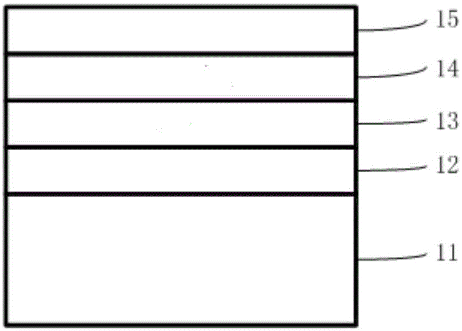
[0053] (1) On the sapphire substrate 11, undoped GaN or AlN buffer layer 12, n-type doped GaN or AlGaN semiconductor material 13, multiple quantum well (MQW) 14, p-type doped GaN or AlGaN are sequentially grown on the sapphire substrate 11 Semiconductor materials15, such as figure 1 shown;

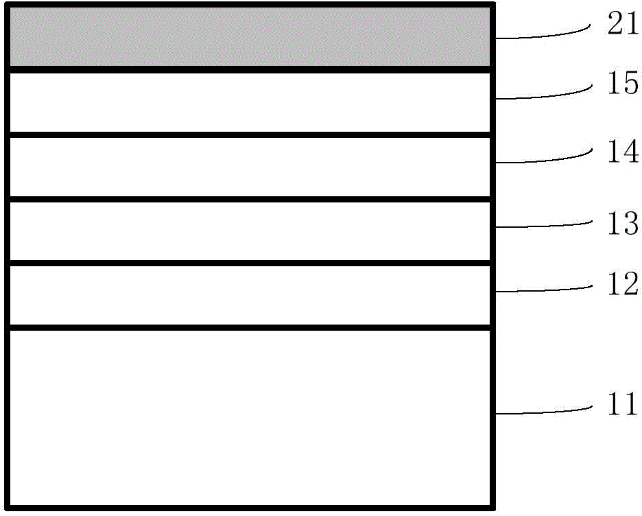
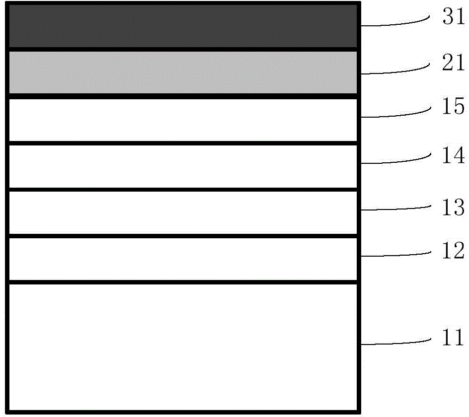
[0054] (2) Forming a transparent conductive layer 21 on the p-type doped GaN or AlGaN semiconductor material 15, such as figure 2 Shown; Adopt sputtering mode to form reflective layer 31 on transparent conductive layer 21, this reflective layer all has higher reflectivity to ultraviolet light and visible light, as image 3 shown.

[0055] (3) Photolithography and dry etching or wet etching are used to process the reflective layer 31, the transparent conductive layer 21, the p-type doped GaN or AlGaN semiconductor material 15, the multiple quantum well (MQW) 14, and the n-type The doped GaN or AlGaN semiconductor material 13 is microfabricated to form periodically or non-periodically d...

Embodiment 2

[0066] A three-dimensional LED light-emitting device includes an LED chip and a heat dissipation substrate. The LED chip is provided with a p-type ohmic contact electrode and an n-type ohmic contact electrode; An insulating layer, a seed layer and a conductive and heat-conducting metal hole core are deposited in sequence; the p-type ohmic contact electrode and the n-type ohmic contact electrode are welded on the conductive and heat-conducting metal hole core through metal wires.

[0067] The LED chip (horizontal structure LED chip) sequentially includes a sapphire substrate, a GaN or AlGaN layer and an n-type doped GaN or AlGaN semiconductor layer from bottom to top; There are n-type ohmic contact electrodes and multi-quantum well light-emitting layers, and p-type doped GaN or AlGaN semiconductor layers, transparent conductive layers and p-type ohmic contact electrodes are sequentially arranged on the multi-quantum well light-emitting layers. The p-type ohmic contact electrode...

Embodiment 3

[0070] A three-dimensional LED light-emitting device includes an LED chip and a heat dissipation substrate. The LED chip is provided with a p-type ohmic contact electrode and an n-type ohmic contact electrode; An insulating layer, a seed layer and a conductive and heat-conducting metal hole core are deposited in sequence; the p-type ohmic contact electrode and the n-type ohmic contact electrode are welded on the conductive and heat-conducting metal hole core through metal wires.

[0071] The LED chip includes an n-type ohmic contact electrode, a GaN or AlGaN layer, an n-type doped GaN or AlGaN semiconductor layer, a multi-quantum well light-emitting layer, a p-type doped GaN or AlGaN semiconductor layer, a transparent Conductive layer, reflective layer and p-type ohmic contact electrode.

[0072] The conductive substrate 81 is used as the p-electrode of the vertical structure LED chip, and the n-electrode 82 is located on the top of the vertical structure LED chip, such as Fig...


PUM


Abstract

The invention relates to a three-dimensional LED luminescent device and belongs to the field of a light emitting diode. The three-dimensional LED luminescent device comprises an LED chip and a radiating substrate, a p type ohmic contact electrode and an n type ohmic contact electrode are arranged on the LED chip; a plurality of electric conduction and heat conduction through holes are formed in the radiating substrate, an insulating layer, a seed layer and an electric conduction and heat conduction metal hole core are deposited on an inner wall of the electric conduction and heat conduction through hole in sequence; the p type ohmic contact electrode is welded to the electric conduction and heat conduction metal hole core. The three-dimensional LED luminescent device has the advantages that the volume of the LED luminescent device is reduced, the luminous efficiency and the heat dispersion are enhanced for the LED luminescent device, and reliability of the LED luminescent device is improved.

Description

technical field [0001] The invention relates to a three-dimensional LED light-emitting device, which belongs to the field of light-emitting diodes. Background technique [0002] LED light-emitting devices can convert about 30% of electrical power into optical power, and the remaining 70% of electrical power is converted into heat energy. Therefore, enhancing the heat dissipation performance of LED light-emitting devices is crucial to improving the performance and reliability of LED light-emitting devices. In applications such as automotive headlights, stage lights, and projectors, high-intensity LED light sources are required. The luminous intensity and luminous flux of the LED can be increased by increasing the driving current of the LED light emitting device and the size of the LED light emitting device. However, as the size of the LED chip increases, it becomes more difficult for the injection current to spread uniformly in the LED chip, and it becomes more difficult to ...

Claims


Application Information

Patent Timeline
Patent Type & Authority Applications(China)
IPC IPC(8): H01L33/48H01L33/62H01L33/64H01L33/00
Inventor 刘胜周圣军郑怀陈飞
Owner WUHAN UNIV
Why Eureka
Try Eureka