Method for producing light emitting diode

a technology of light-emitting diodes and diodes, which is applied in the direction of liquid surface applicators, coatings, semiconductor devices, etc., can solve the problems of significant limit of application, unsatisfactory current spreading, and bubbles at the interface, so as to improve current spreading, reduce resistance, and increase the effect of emitting efficiency

Inactive Publication Date: 2005-02-10
NAT SCI COUNCIL
View PDF1 Cites 5 Cited by
  • Summary
  • Abstract
  • Description
  • Claims
  • Application Information

AI Technical Summary

Benefits of technology

[0009] An object of the present invention is to provide a method for producing a light emitting diode (LED), so that the LED exhibits higher emitting efficiency, lower resistance and better current spreading than a conventional LED.

Problems solved by technology

However, GaAs can absorb visible light emitted from double hetero-junction structure and GaP can absorb yellow-green wavelength, which significantly limit the application thereof.
Unfortunately, the adhesives easily result in bubbles at the interface.
Additionally, current spreading is not satisfying by such methods, unless the cladding layer adjacent to the transparent substrate is thick enough, or a GaP layer used for oxidation barrier is thicker than 3 μm, which certainly increases the cost.

Method used


Image

  • Method for producing light emitting diode
  • Method for producing light emitting diode
  • Method for producing light emitting diode

Examples


first embodiment

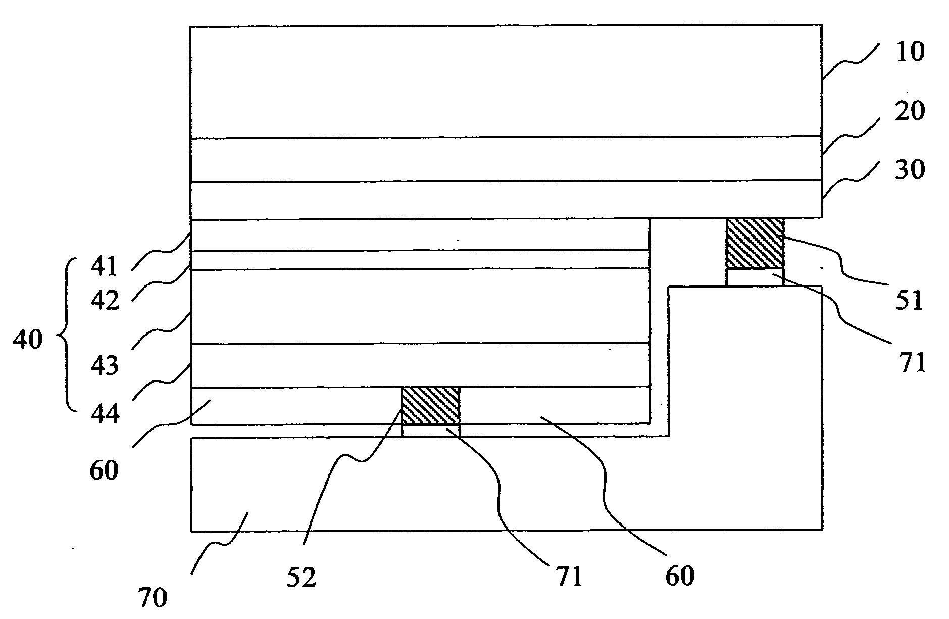
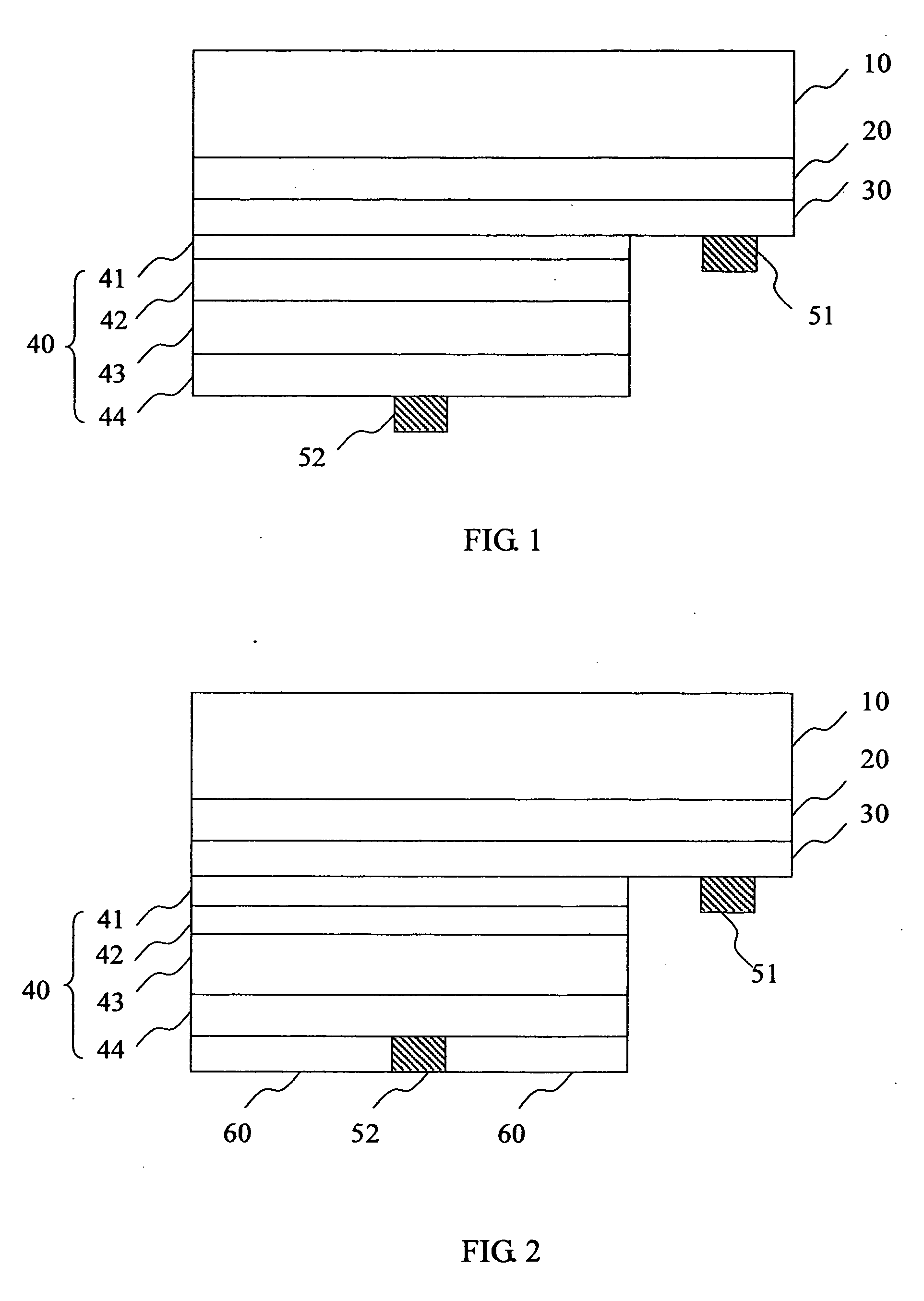
[0025] Referring to FIG. 1, the first embodiment in accordance with the present invention includes a transparent window 10 made from glass, a transparent conductive film 20 made from ITO, a p-type ohmic contact layer 30, an LED epitaxial layer 40 formed on partial surface of the p-type ohmic contact layer 30, and a positive electrode 51 formed on other area of the p-type ohmic contact layer 30. The LED epitaxial layer 40 primarily includes an active layer 43 of undoped AlGaInP, wherein a front surface and a back surface are defined. Between the front surface and the transparent conductive film 20, a second cladding layer 42 of p-type AlGaInP and an oxidation barrier 41 of GaP for preventing the cladding layer 42 from oxidization are formed. On the back surface, a first cladding layer 44 of n-type AlGaInP is formed, on partial area of which the negative electrode 52 is formed.

[0026] The transparent conductive film 20 can be made from other materials than ITO. A thin film made from an...

second embodiment

[0028]FIG. 2 shows a cross section view of the second embodiment, in which a reflective layer 60 is coated on the first cladding layer 44. Therefore, the LED in this embodiment can exhibit higher brightness than that shown in FIG. 1, because all light beams emit from the front side of the LED.

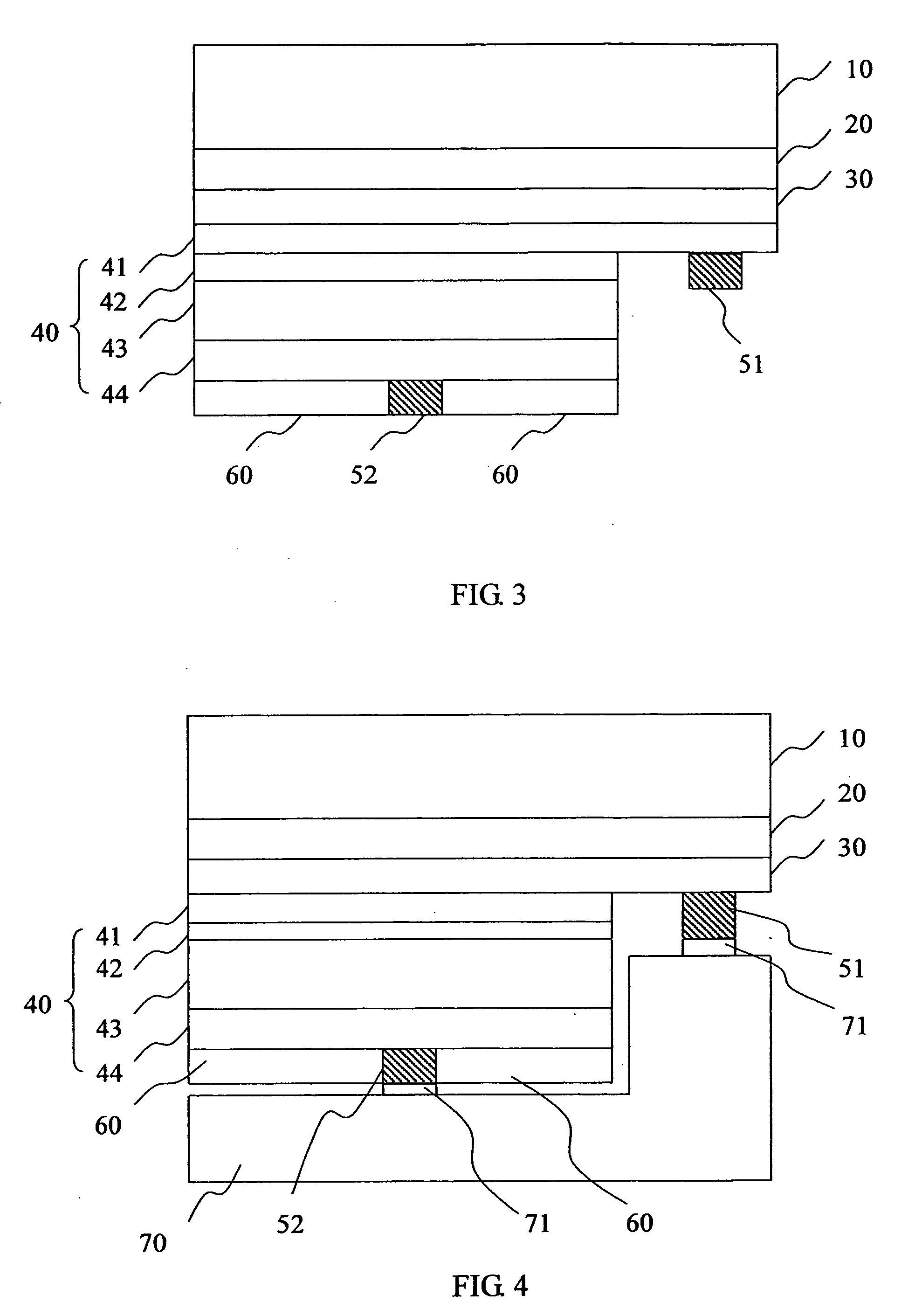
[0029]FIG. 3 shows the third embodiment, which is similar to the second embodiment but the positive electrode 51 is moved to the GaP oxidation barrier 41 from the ohmic contact layer 30.

[0030]FIG. 4 shows the forth embodiment, which is similar to the second embodiment but a heat-transferring set 70 is adhered to the electrodes 51, 52 with wire-bonding glue 71 during wire binding. Accordingly, heat caused by electric power can be brought away, and therefore life of the device is elongated.

[0031]FIGS. 5 and 6 show the manufacturing process of the forth embodiment. First, on a GaAs substrate 80, the first cladding layer 44, the active layer 43, the second cladding layer 42, the oxidation barrier...


PUM


Abstract

The present invention discloses a method for producing an LED (light emitting diode), in which a transparent conductive film is formed between a transparent window and the front surface of a LED epitaxial layer. The transparent conductive film can be oxides, nitrides or fluorides of metals. The transparent conductive film can be preliminarily formed on one of the transparent window and the LED epitaxial layer or both of them by a suitable process, for example, thermal pressure. By involving the transparent conductive film, current spreading is improved and resistance is reduced because of larger cross section areas provided, particularly compared with the conventional spin on glass or polymer adhesives. Additionally, light-emitting efficiency can be improved since the conventional opaque substrate, such as a GaAs substrate.

Description

CROSS REFERENCE [0001] The present Application is a Division of co-pending U.S. application Ser. No. 10 / 405,811 by the same inventors filed on Mar. 31, 2003.BACKGROUND OF THE INVNETION [0002] 1. Field of the Invention [0003] The present invention relates to a method for producing a light emitting diode (LED), and particularly to a method for producing a light emitting diode including a transparent window and a transparent conductive film. [0004] 2. Description of the Related Prior Art [0005] General processes for fabricating LEDs can be divided into up stream, middle stream and down stream. In the up stream, LPE (Liquid Phase Epitaxy), MBE (Molecular Beam Epitaxy) and MOVPE (Metal Organic Vapor Phase Epitaxy) are usually applied to producing single chips or epitaxial chips. In the middle stream, mask, dry or wet etching, vacuum vapor deposition and cutting are applied to forming dice. In the down stream, dice are placed on lead frames, and finally packaged as lamps, digit displays, ...

Claims


Application Information

Patent Timeline
Patent Type & Authority Applications(United States)
IPC IPC(8): B05D5/06H01L21/00H01L21/311H01L31/0203H01L33/00H01L33/42
CPCH01L33/42H01L33/0079H01L33/0093
Inventor HORNG, RAY-HUAWU, TUNG-HSINGHUANG, SHAO-HUACHIU, CHI-YING
Owner NAT SCI COUNCIL
Why Eureka
Try Eureka