Photoresist, photolithography method using the same, and method for producing photoresist

a photolithography and photoresist technology, applied in the field of photoresist, can solve the problems of shortening the laser wavelength, miniaturizing equipment, and the thickness of the photoresist film cannot be as thick as those in the conventional methods, and achieves the effects of reducing pattern edge roughness, improving pattern rectangularity, and high light utilization efficiency

Inactive Publication Date: 2005-02-01
CANON KK
View PDF7 Cites 20 Cited by
  • Summary
  • Abstract
  • Description
  • Claims
  • Application Information

AI Technical Summary

Benefits of technology

The present invention provides a positive photoresist that can improve pattern rectangularity and reduce pattern edge roughness by reducing reflection from the substrate. This results in a high light utilization efficiency even with a small layer thickness of the photoresist layer for image formation. The invention also provides a photolithography method using near-field exposure to form a photoresist layer for image formation.

Problems solved by technology

The patent text discusses the problem of pattern edge roughness in the near-field exposure method. The conventional commercial photoresists used in this method have a low efficiency for light utilization, resulting in poor pattern edge resolution and adverse effects on device fabrication. The text proposes a method to improve the efficiency of light utilization by using a specific g-line or i-line photoresist that matches the pattern formation method. However, the thickness of the photoresist film and the light passing through the microaperure of a probe can cause pattern edge roughness and the absence of a sharp pattern edge in the resulting patterns. The text also discusses the use of a commercial g-line positive photoresist with a high-speed laser and an aligner to expose patterns. The text aims to address these issues by proposing a method to improve the efficiency of light utilization in the near-field exposure method.

Method used


Image

  • Photoresist, photolithography method using the same, and method for producing photoresist
  • Photoresist, photolithography method using the same, and method for producing photoresist
  • Photoresist, photolithography method using the same, and method for producing photoresist

Examples


example 1

The diazide compound containing a photosensitive compound 1,2-naphthoquinone diazide-5-sulfonic acid ester as the main component in an amount corresponding to 80 parts by weight per 100 parts by weight of a photoresist base resin (alkali-soluble novolak resin) and PGMEA as solvent were added to a commercial positive photoresist for semiconductor production containing 30 parts by weight of a photosensitive compound (naphthoquinone diazide) per 100 parts by weight of the photoresist base resin, and the resultant was mixed to prepare a positive photoresist for near-field exposure having a viscosity of 5 cP. The absorption coefficient of the photoresist was measured and found to be 1.0.

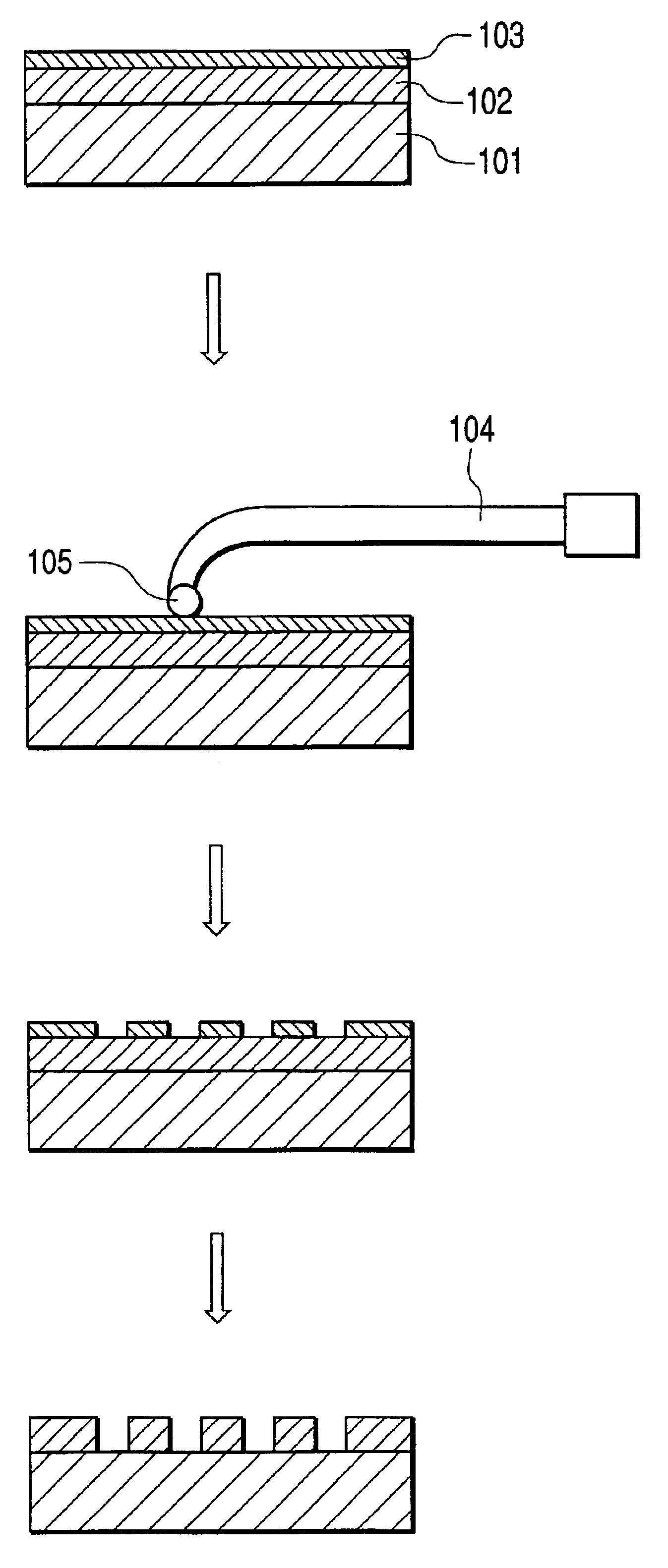
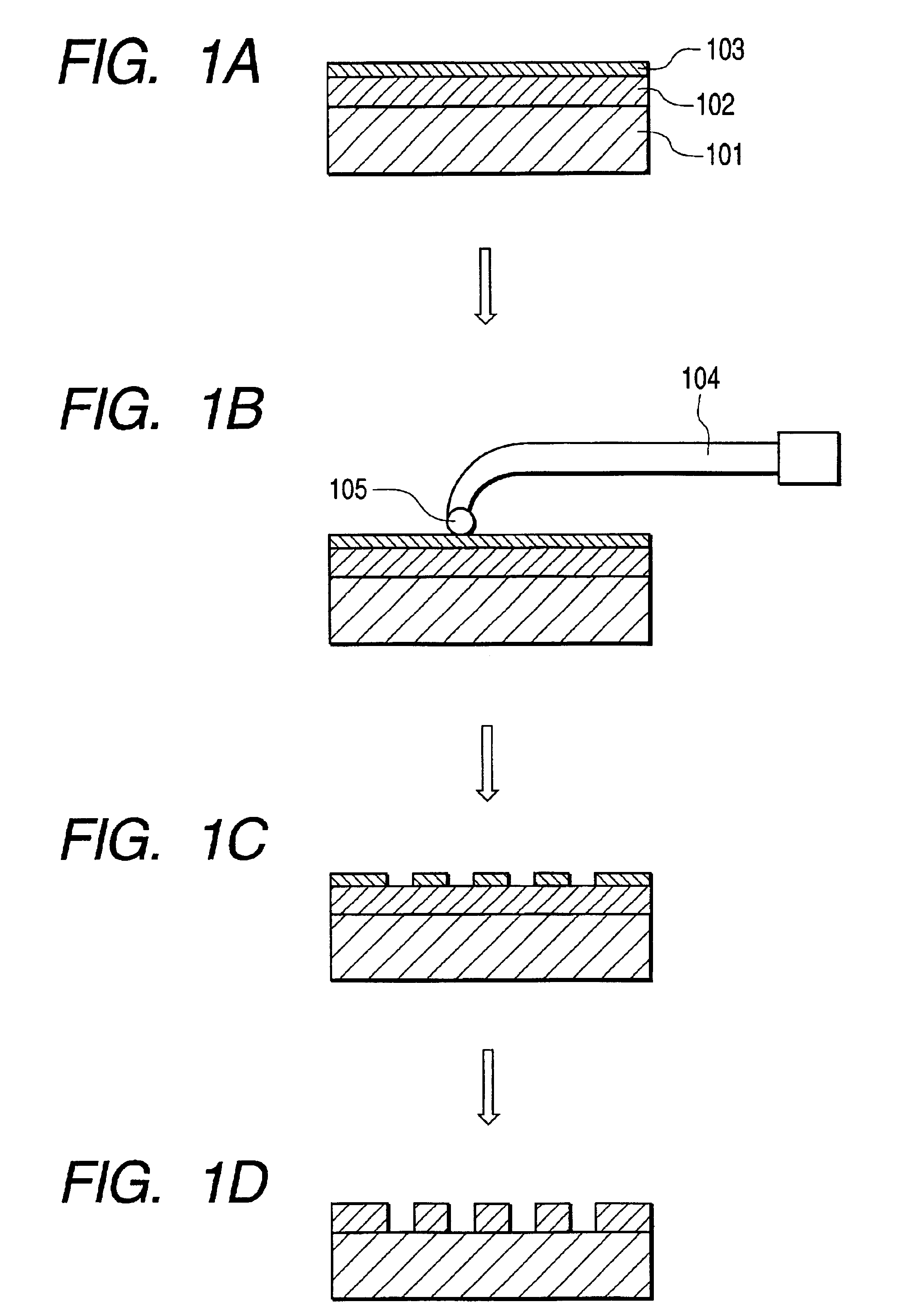
A substrate was spin-coated with the positive photoresist for near-field exposure in a sealed space to form a photoresist layer for image formation.

A glass substrate 101 having a deposited Cr layer 102 of 30 nm in thickness was used as the substrate (see FIG. 1A). Then the Cr layer was spin-coated with th...

example 2

The diazide compound containing a photosensitive compound 1,2-naphthoquinone diazide-5-sulfonic acid ester as the main component in an amount corresponding to 80 parts by weight per 100 parts by weight of the alkali-soluble novolak resin as a base resin (molecular weight distribution (Mw / Mn) is 2.5) was added to a photoresist containing 30 parts by weight of a photosensitive compound (naphthoquinone diazide) per 100 parts by weight of the base resin, and further GPMEA as solvent was added thereto, and the resultant was mixed to prepare a positive photoresist for near-field exposure having a viscosity of 5 cP. The absorption coefficient of the photoresist was measured and found to be 1.0.

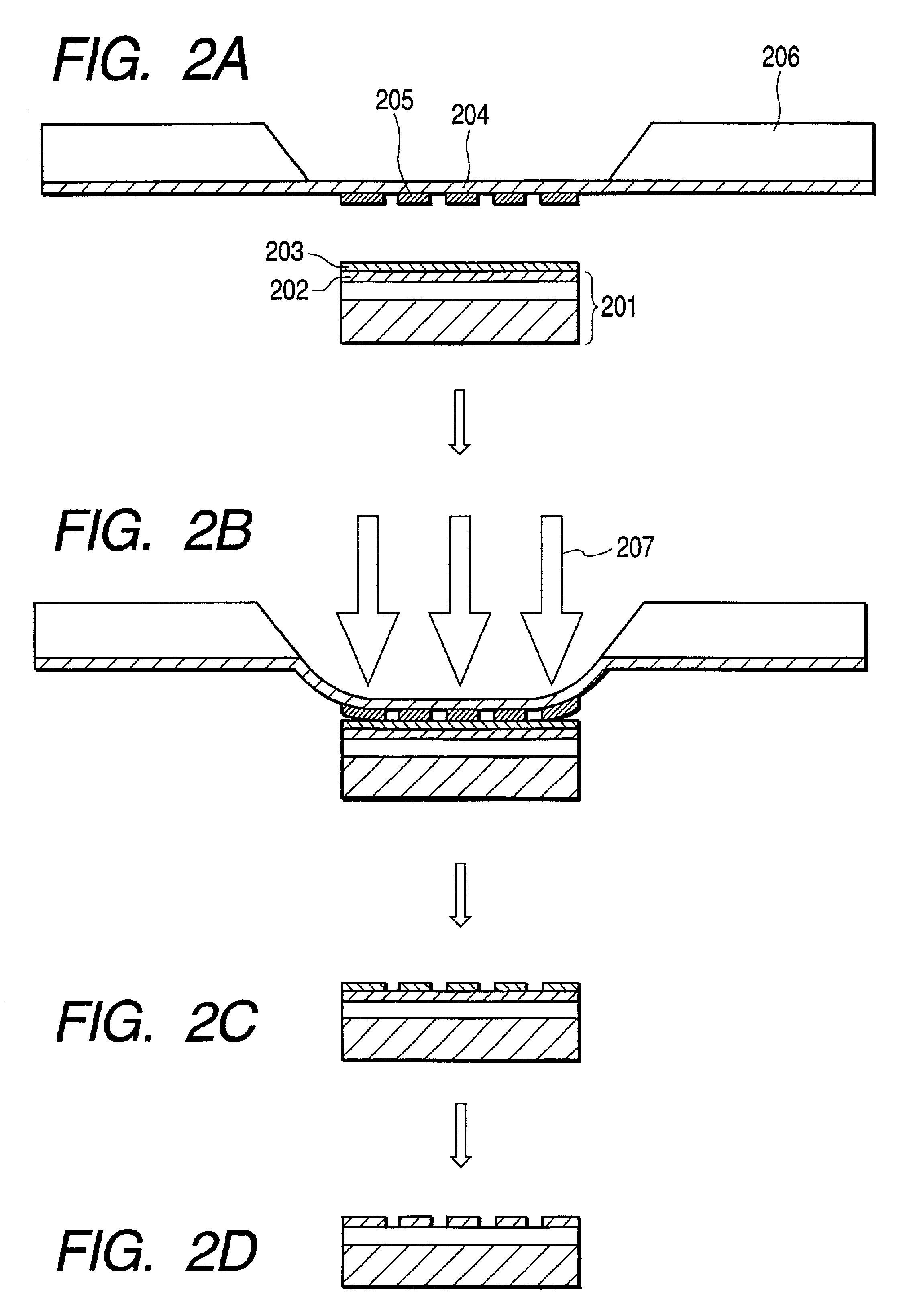
A substrate was spin-coated with the positive photoresist for near-field exposure under the spin-coating condition 7,000 rpm×60 sec in a sealed space to form a photoresist layer for image formation. An SOI (Silicon On Insulator) substrate 201 having an upper Si layer 202 of 50 nm in thickness was use...

example 3

The diazide compound containing a photosensitive compound 1,2-naphthoquinone diazide-5-sulfonic acid ester as the main component in an amount corresponding to 80 parts by weight per 100 parts by weight of a base resin (alkali-soluble novolak resin) was added to a commercial Si-containing photoresist for semiconductor production including 15 parts by weight of a photosensitive compound (naphthoquinone diazide) per 100 parts by weight of the base resin and further GPMEA as solvent was added thereto, and the resultant was mixed to prepare a positive photoresist for near-field exposure having a viscosity of 5 cP. The absorption coefficient of the photoresist was measured and found to be 1.0.

An SOI (Silicon On Insulator) substrate 303 having an upper Si layer of 300 nm in thickness was used as the substrate. In order to apply the multilayer photoresist method, a commercial positive photoresist was applied to the upper Si layer by using a spin coater, and then the substrate was hard-baked...


PUM


Abstract

There is provided a positive photoresist for near-field exposure excellent in light utilization efficiency even with small layer thickness of the photoresist layer for image formation, and allowing for reduced pattern edge roughness, and a photolithography method including a step of exposing by the near-field exposure the photoresist layer for image formation made thereof. In a positive photoresist containing an alkali-soluble novolak resin and a quinone diazide compound, the film thickness of the photoresist at the time of exposure is not larger than 100 nm, and the absorption coefficient of the photoresist α (μm−1) for the exposure light is such that 0.5≦α≦7.

Description


Claims


Application Information

Patent Timeline
Owner CANON KK
Why Eureka
Try Eureka