Semiconductor integrated circuit with shortened pad pitch

a technology of integrated circuits and semiconductors, applied in the direction of semiconductor/solid-state device testing/measurement, basic electric elements, instruments, etc., can solve the problems of failure of test and unsuitability, and achieve the effects of shortening the pitch of the pad, increasing the bandwidth of signal input/output, and increasing the pad density

Inactive Publication Date: 2005-02-01
SOCIONEXT INC
View PDF8 Cites 11 Cited by
  • Summary
  • Abstract
  • Description
  • Claims
  • Application Information

AI Technical Summary

Benefits of technology

In the semiconductor integrated circuit described above, two types of pads are mixed and arranged in line, one type being the first pads for probe contact having a width that enables a probe needle to secure proper contact, and the other type being the second pads having a narrower width. This makes it possible to increase pad density by shortening a pad pitch compared to when all the pads arranged in line have the same width as the pads for probe contact. Further, the switch circuit is provided such that input / output signals corresponding to the second pads having narrower width are input / output through the first pads for probe contact. During test operations, the probe needles are brought into contact with the pads for probe contact, and the switching state of the switch circuit is controlled so that all the signals corresponding to the narrower pads as well as the pads for probe contact are input / output through the pads for probe contact. In this manner, the pitch of pads on the semiconductor integrated circuit is shortened to increase the bandwidth of signal input / output while maintaining secure contact between the probe needles and the pads.

Problems solved by technology

Otherwise, improper contact will results in a failure of the test.
This is not desirable, however, because of problems associated with the durability of needles.

Method used


Image

  • Semiconductor integrated circuit with shortened pad pitch
  • Semiconductor integrated circuit with shortened pad pitch
  • Semiconductor integrated circuit with shortened pad pitch

Examples


Embodiment Construction

In the following, embodiments of the present invention will be described with reference to the accompanying drawings.

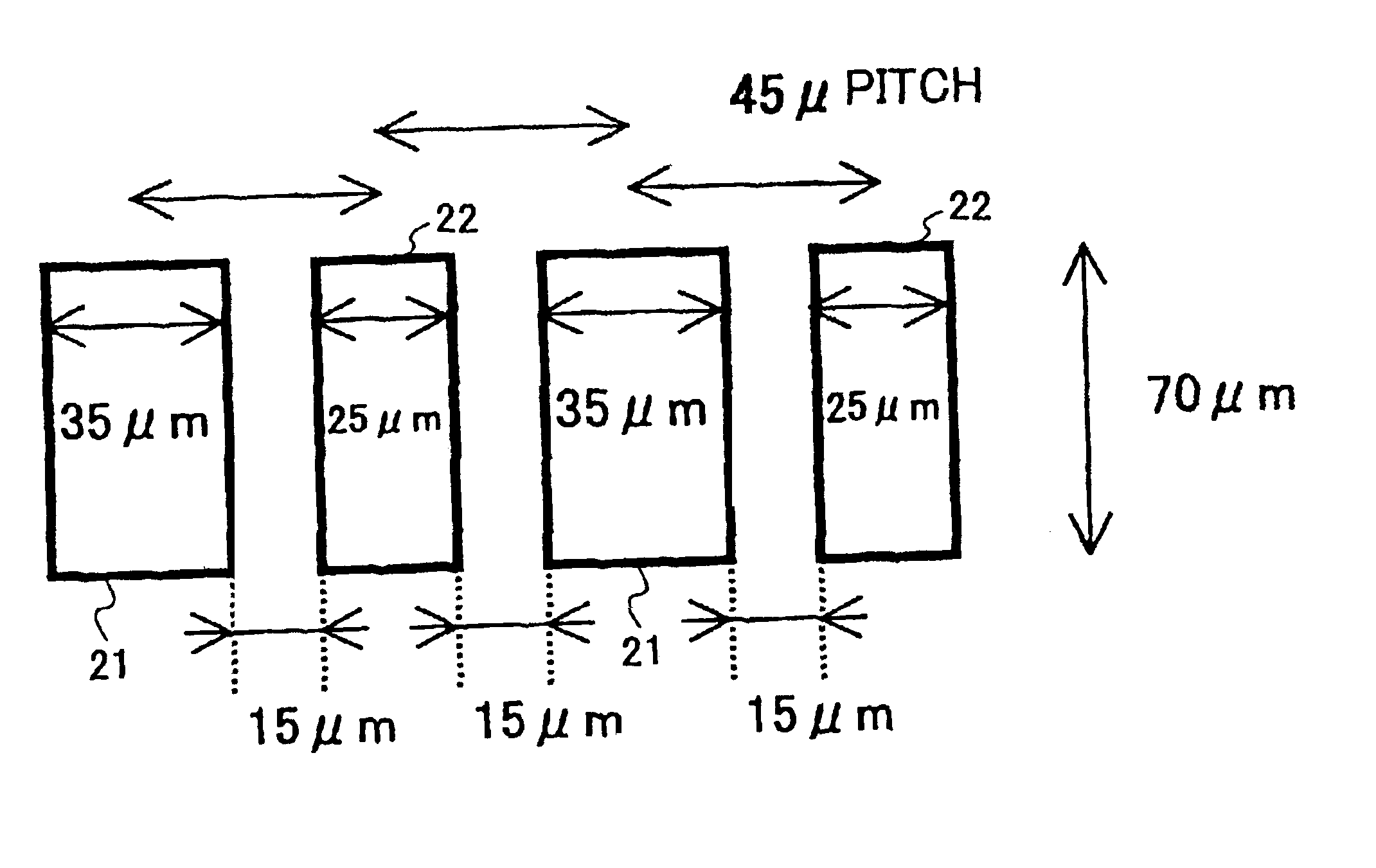
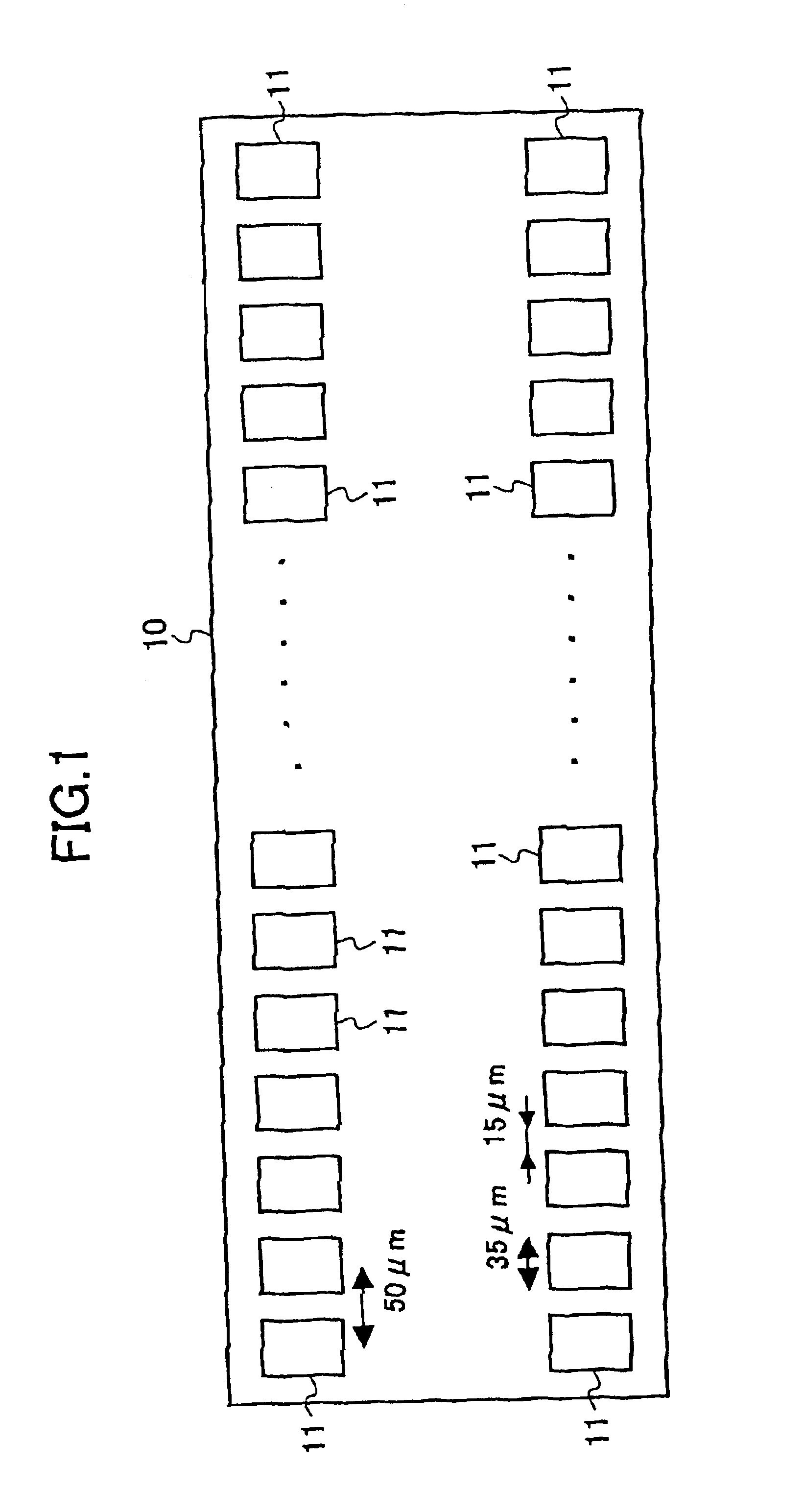
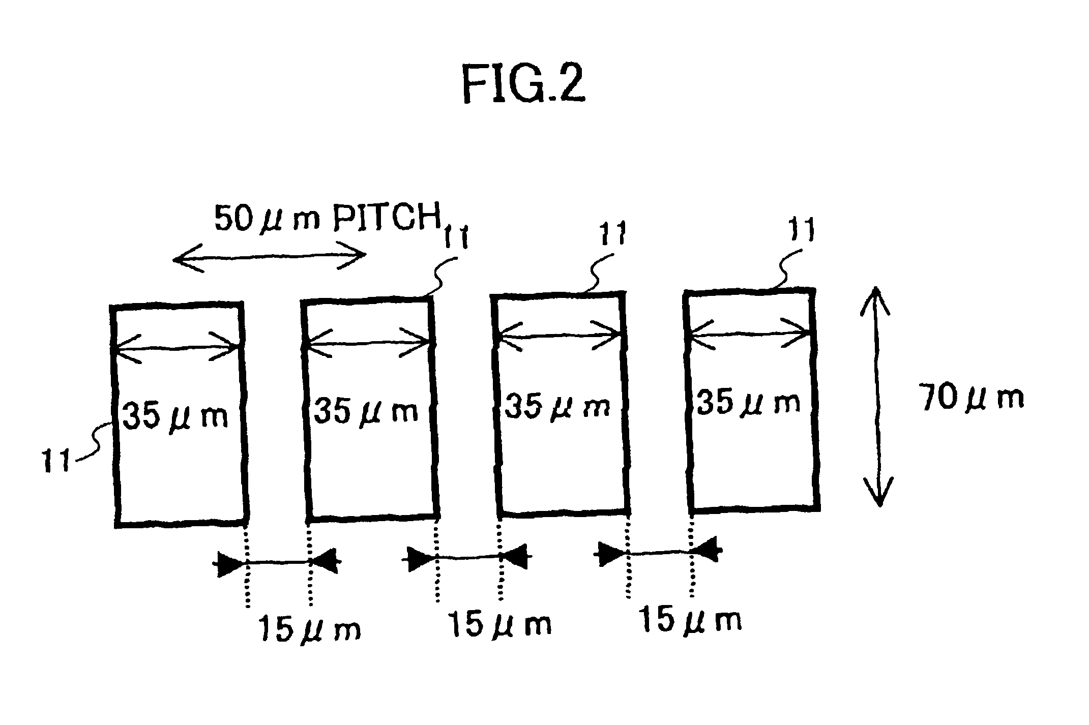
FIG. 3 is an illustrative drawing showing a pad arrangement on a semiconductor integrated circuit according to the present invention. A semiconductor integrated circuit 20 of FIG. 3 is a driver IC or the like that drives a liquid crystal display panel, for example. A plurality of first pads 21 and a plurality of second pads 22 are arranged in turn to form a line, and two rows are provided in such a manner. FIG. 4 is an example of the size and layout of the first pads 21 and the second pads 22.

As shown in FIG. 4, each of the first pads 21 has a rectangular shape measuring 70 micrometers by 35 micrometers. The second pads 22 are smaller than the first pads 21, and each has a rectangular shape measuring 70 micrometers by 25 micrometers. The first pads 21 and the second pads 22 are situated in turn such that the first pads 21 come next to the second pads 22. Intervals bet...


PUM


Abstract

An semiconductor integrated circuit includes a plurality of first pads having first size, a plurality of second pads having second size smaller than the first size, a switch circuit which couples the first pads to respective first core circuits in a first switching state, and couples the first pads to respective second core circuits in a second switching state, the second core circuits being connected to the second pads, wherein the first pads and the second pads are mixed and arranged in line.

Description

CROSS-REFERENCE TO RELATED APPLICATIONSThe present application is based upon and claims the benefit of priority from the prior Japanese Patent Application No. 2002-140078 filed on May 15, 2002, with the Japanese Patent Office, the entire contents of which are incorporated herein by reference.BACKGROUND OF THE INVENTION1. Field of the InventionThe present invention generally relates to semiconductor integrated circuits, and particularly relates to a semiconductor integrated circuit having pads thereof arranged in line.2. Description of the Related ArtLSIs (larges-scale semiconductor integrated circuits) are provided with pads for the purpose of inputting / outputting signals from / to the exterior. As a single LSI chip is required to have an increased number of functions, the number of pads also increases due to an increase in the number of signal inputs / outputs. As the chip size decreases in response to improved circuit density, the size and pitch of pads need to be decreased in accorda...

Claims


Application Information

Patent Timeline
Patent Type & Authority Patents(United States)
IPC IPC(8): G01R31/28H01L21/60H01L21/02H01L23/50H01L21/66H01L23/48H01L21/822H01L21/70H01L23/52H01L21/82H01L27/04H01L31/00
CPCG01R31/2884H01L24/06H01L22/32H01L2224/05553H01L2924/01002H01L2924/01076H01L2924/01005H01L2924/01006H01L2924/01033H01L2924/01082H01L2924/14H01L2924/01004G11C29/00
Inventor SHIGIHARA, TAKEO
Owner SOCIONEXT INC
Why Eureka
Try Eureka