Low-loss waveguide and method of making same

Inactive Publication Date: 2005-02-01
MASSACHUSETTS INST OF TECH
View PDF12 Cites 48 Cited by
  • Summary
  • Abstract
  • Description
  • Claims
  • Application Information

AI Technical Summary

Benefits of technology

[0010]The invention provides a new waveguide fabrication method that involves a waveguide patterning process, followed by smoothing of the waveguide core surface. The invention provides a method of reducing the scattering losses in planar waveguide by subjecting the already-fabricated waveguide

Problems solved by technology

Yet there has been no prior art on reducing the scattering losses by subjecting high index difference waveguides to a smoothing process after the wavegu

Method used


Image

  • Low-loss waveguide and method of making same
  • Low-loss waveguide and method of making same
  • Low-loss waveguide and method of making same

Examples


Embodiment Construction

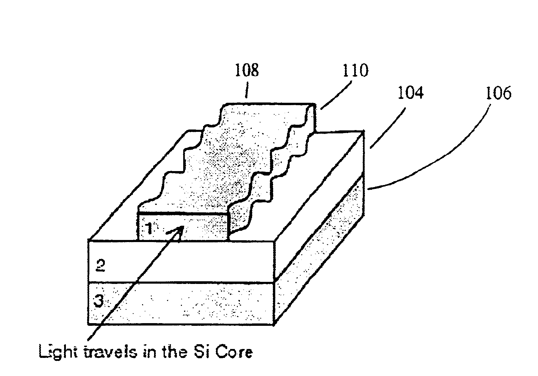
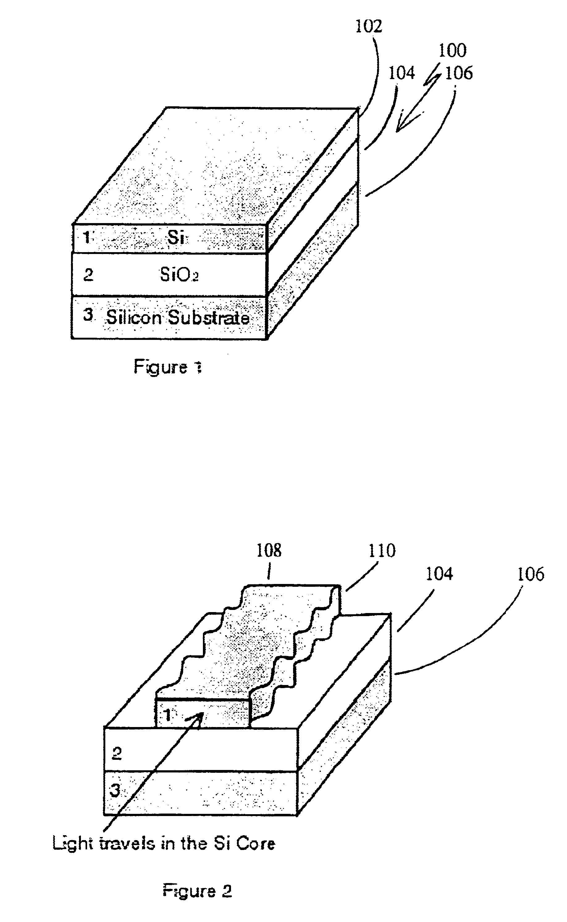
[0017]An exemplary embodiment of the invention provides an oxidation smoothing technique that reduces the roughness at the core / cladding interfaces of Si / SiO2 waveguide. FIG. 1 is a perspective block diagram of an initial SOI platform 100 on which a waveguide is formed. A top silicon layer 102 will be made into a waveguide core while a SiO2 layer 104 will become an undercladding layer. A silicon substrate 106 is provided for mechanical support.

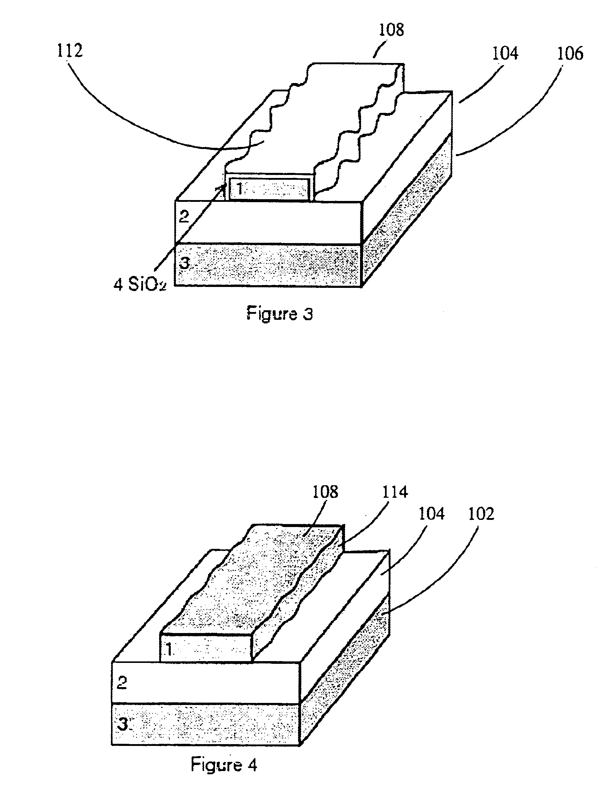
[0018]FIG. 2 is a perspective block diagram of the platform including a waveguide core 108 after a typical patterning process including photolithography and etching of the layer 102. The sidewall roughness 110 of the core 108 is due to the waveguide patterning process. This roughness is responsible for scattering loss in the waveguide. The core 108 is then subjected to oxidizing agents, such as O2 or H2O gases at an elevated temperature. The surfaces of the core will react with the oxidizing agents and form a coating layer of SiO2 112, as show...


PUM

PropertyMeasurementUnit
Temperatureaaaaaaaaaa

Abstract

A method of reducing the scattering losses that involves smoothing of the core/cladding interface and/or change of waveguide geometry in high refractive index difference waveguides. As an example, the SOI-based Si/SiO2 waveguides are subjected to an oxidation reaction at high temperatures, after the waveguide patterning process. By oxidizing the rough silicon core surfaces after the patterning process, the core/cladding interfaces are smoothened, reducing the roughness scattering in waveguides.

Description

[0002]This application claims priority from provisional application Ser. No. 60 / 217,167 filed Jul.10, 2000, and claims the benefits of 60 / 217,167 filed Jul. 10, 2000.[0003]This invention was made with government support under Grant No. DMR-9808941 awarded by the National Science Foundation. The government has certain rights in the invention.BACKGROUND OF TH INVENTION[0004]The invention relates to the field of optical waveguides, and the method of manufacturing waveguides.[0005]Roughness scattering is one of the major sources of transmission loss in planar waveguides. The roughness at the core / cladding interface, arising from the waveguide patterning process, is responsible for such a scattering. Several methods are possible to reduce the scattering losses in planar waveguides. Reduction of scattering loss by annealing the waveguide at high temperature, after the waveguide patterning process, has been previously reported by Kashimura et al. in Japanese Journal of Applied Physics, Vol...

Claims


Application Information

Patent Timeline
IPC IPC(8): G02B6/13G02B6/132G02B6/122G02B6/12
CPCG02B6/122G02B6/132G02B6/13G02B2006/12176G02B6/12
Inventor LEE, KEVIN K.LIM, DESMOND R.WADA, KAZUMIKIMERLING, LIONEL C.
Owner MASSACHUSETTS INST OF TECH
Why Eureka
Try Eureka