Wafer level package having a side package

a technology of side package and wafer, which is applied in the direction of semiconductor devices, semiconductor/solid-state device details, electrical equipment, etc., can solve the problems of wafer level packaging, inability of the process to package and the semiconductor chip not having a package body surrounding all sides of the semiconductor chip is vulnerable to physical damag

Inactive Publication Date: 2005-02-08
SAMSUNG ELECTRONICS CO LTD
View PDF4 Cites 66 Cited by
  • Summary
  • Abstract
  • Description
  • Claims
  • Application Information

AI Technical Summary

Benefits of technology

With the descriptions mentioned above along with other feature and advantages, the outline will be more clearly understood from the following detailed description taken in conjunction with the accom...

Problems solved by technology

However, drawbacks do exist with wafer level packaging.
Most notably, the inability of the process to package all sides of the semiconductor chip.
A semiconductor chip not having a package body surrounding all sides of the semiconductor chip is vulnerable to physical damage, for example, from physical contact w...

Method used


Image

  • Wafer level package having a side package
  • Wafer level package having a side package
  • Wafer level package having a side package

Examples


Embodiment Construction

Embodiments of the present invention are described below with reference to the accompanying drawings.

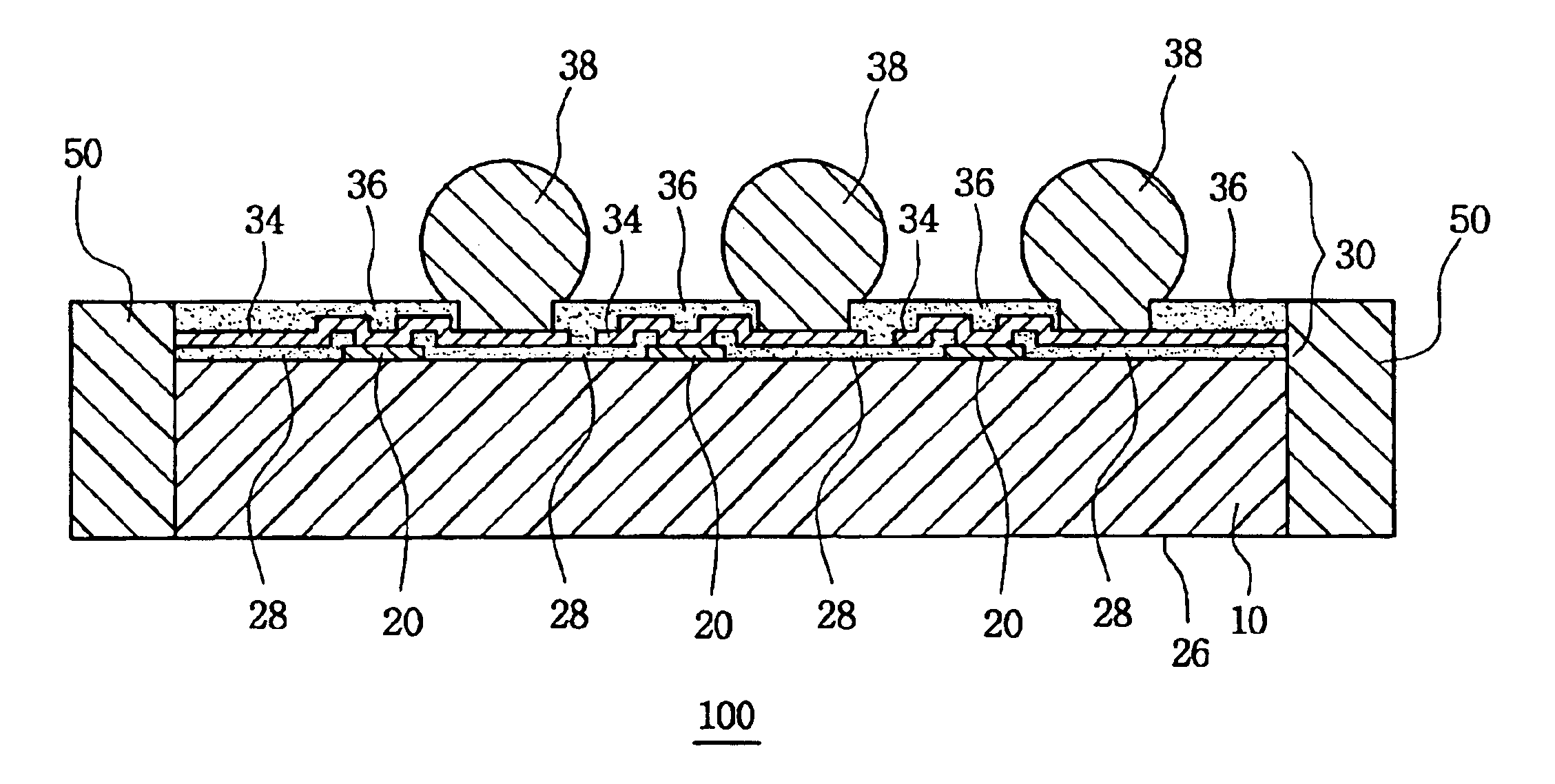
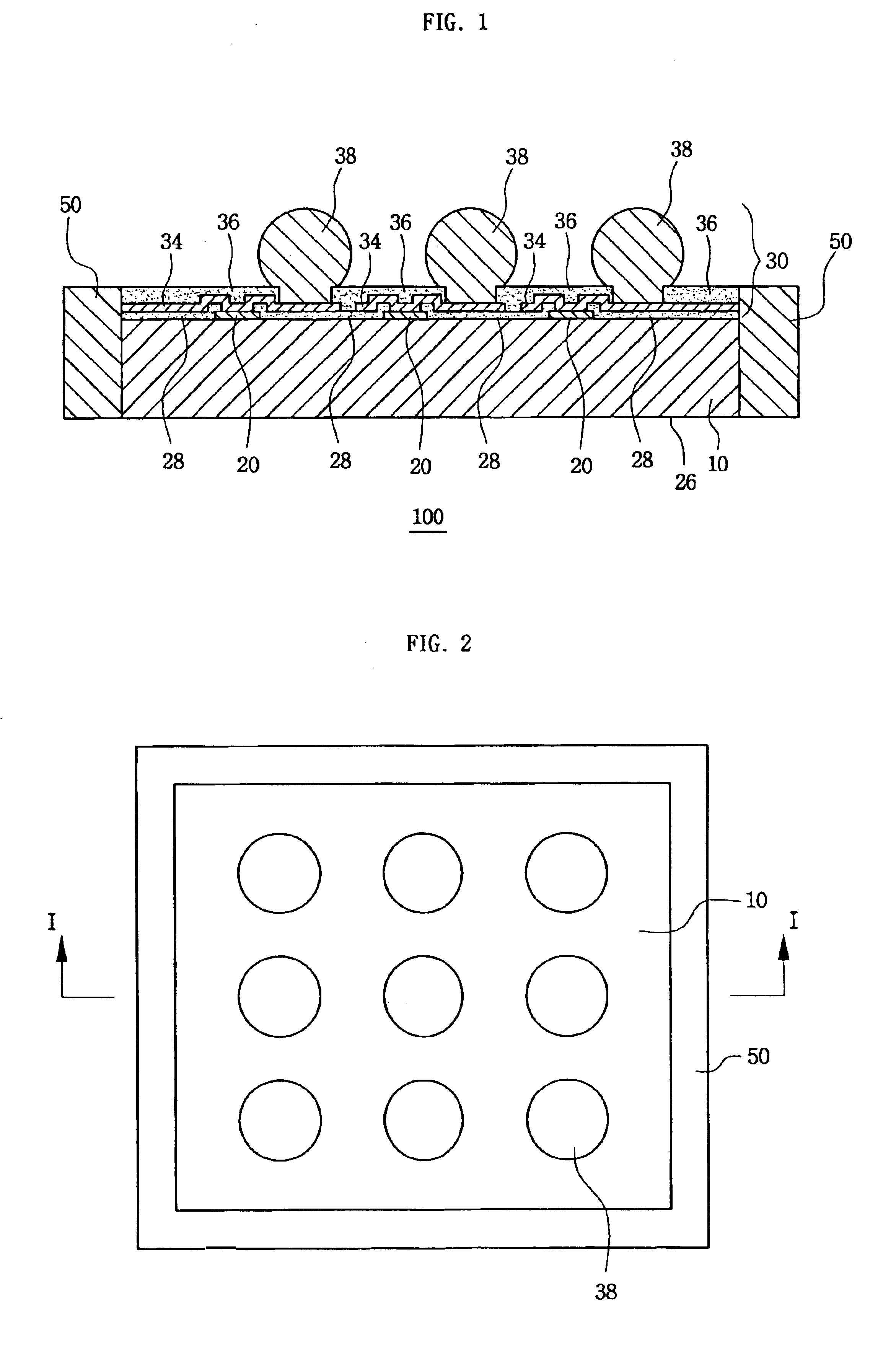
FIG. 1 is a cross sectional view showing a wafer level package according to the present invention.

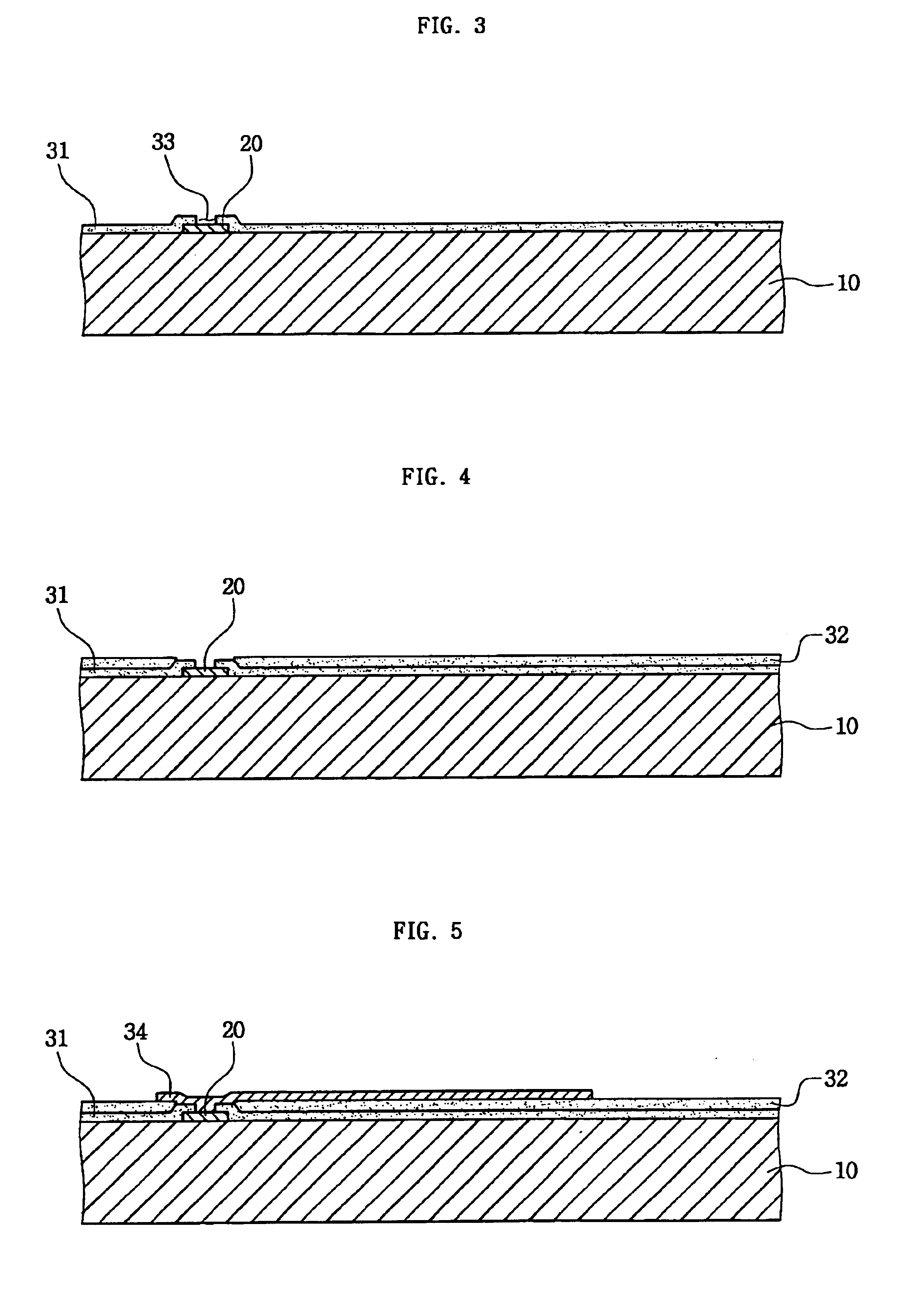
A wafer level package 100 according to the present invention includes a semiconductor chip 10, a package pattern 30, and a package body 50 which is formed on the side surface of semiconductor chip 10. Semiconductor chip 10 includes circuit elements (not shown) which are integrated on semiconductor chip 10 by the wafer fabrication process. These circuit elements are referred to as “on-chip circuits” and are selected based on the electrical characteristics and the functions of semiconductor chip 10. Metal electrode pads 20 formed on the active surface of semiconductor chip (the top surface of semiconductor chip 10 as shown in FIG. 1) provide electrical connections to electrically connect the on-chip circuits to external devices (not shown).

Package pattern 30 formed on the active surface of...


PUM


Abstract

A method of manufacturing a wafer level package includes forming a semiconductor wafer including semiconductor chips, and forming a package body on the sides of each semiconductor chip. The package body is formed by forming a space between each semiconductor chip and potting a package material in the space, which can be a mold resin. The wafer is then separated into separate semiconductor chips by cutting through the package body.

Description

BACKGROUND OF THE INVENTIONThe present invention relates to a semiconductor chip packaging technology, and more particularly to a wafer level package having a side package.Semiconductor chip packages provide input and output connections to a semiconductor chip for an external device, as well as physical protection for the semiconductor chip. The wafer level package is one type of semiconductor chip package. The wafer level package is a package formed on a semiconductor wafer, rather than on a die (a “die” refers to a semiconductor chip that has been separated from the wafer). Forming a wafer level package on a wafer has the advantages of providing more complete integration of the package functions and the semiconductor chip functions, improving the thermal and electrical characteristics of the semiconductor chips, and decreasing the size of the semiconductor chip package. Additionally, since the wafer level package is formed in a single process, the price to manufacture the semicond...

Claims


Application Information

Patent Timeline
IPC IPC(8): H01L21/56H01L21/02H01L21/301H01L23/12H01L23/02
CPCH01L21/56H01L2924/0002H01L2924/00H01L23/02
Inventor SONG, YOUNG HEESON, MING YOUNGHA, WOONG KY
Owner SAMSUNG ELECTRONICS CO LTD
Why Eureka
Try Eureka