Electrostatic discharge depolarization using high density plasma

a technology of electrostatic discharge and high density plasma, which is applied in the direction of circuit arrangement, nuclear engineering, therapy, etc., can solve the problems of undesirable adhesion of the wafer to the pad, observable misalignment of the wafer and the pad, and no general application protocol for neutralizing the buildup of electrical charges within the vacuum region of the tools themselves. , to achieve the effect of reducing the polarization of the tool portion and reducing the electrostatic discharg

Inactive Publication Date: 2005-02-08
ADVANCED MICRO DEVICES INC
View PDF13 Cites 2 Cited by
  • Summary
  • Abstract
  • Description
  • Claims
  • Application Information

AI Technical Summary

Benefits of technology

The aforementioned needs are addressed by the present invention. Accordingly a method for reducing electrostatic discharge (ESD) by depolarization of a polarized portion of a fabrication tool of is provided. The method includes the step of selectively exposing the portion of a fabrication tool to a plasma for a selected time interval. The duration of the exposure time interval is sufficient to reduce the polarization of the tool portion whereby interference with a motion of a device being processed by the tool is not observed.

Problems solved by technology

These control strategies are typically employed in the fabrication facilities external to the tools, however, currently, there are no generally applied protocols for neutralizing the buildup of electrical charges within the vacuum regions of the tools themselves.
As the pad becomes electrically polarized, which may bear a surface voltage on the order of 10 kilo volts, an undesirable adhesion of the wafer to the pad may be observed.
During the wafer loading process, the electrostatic forces between the wafer and the pad may result in an observable misalignment of the wafer and pad since the wafer cannot slide freely on the pad.
The misalignment is detected by the wafer handling equipment and processing of the wafers cannot be performed under these circumstances.
Retrieving the misaligned wafer is usually time consuming since it has to be removed manually from the pad.
In such cases, the wafer may be popped up from the wafer pad causing it to be offset from its normal position and the wafer transportation mechanism cannot retrieve the wafer automatically.
In either cases, the product wafer is at risk of breakage and production time wasted.

Method used


Image

  • Electrostatic discharge depolarization using high density plasma
  • Electrostatic discharge depolarization using high density plasma
  • Electrostatic discharge depolarization using high density plasma

Examples


Embodiment Construction

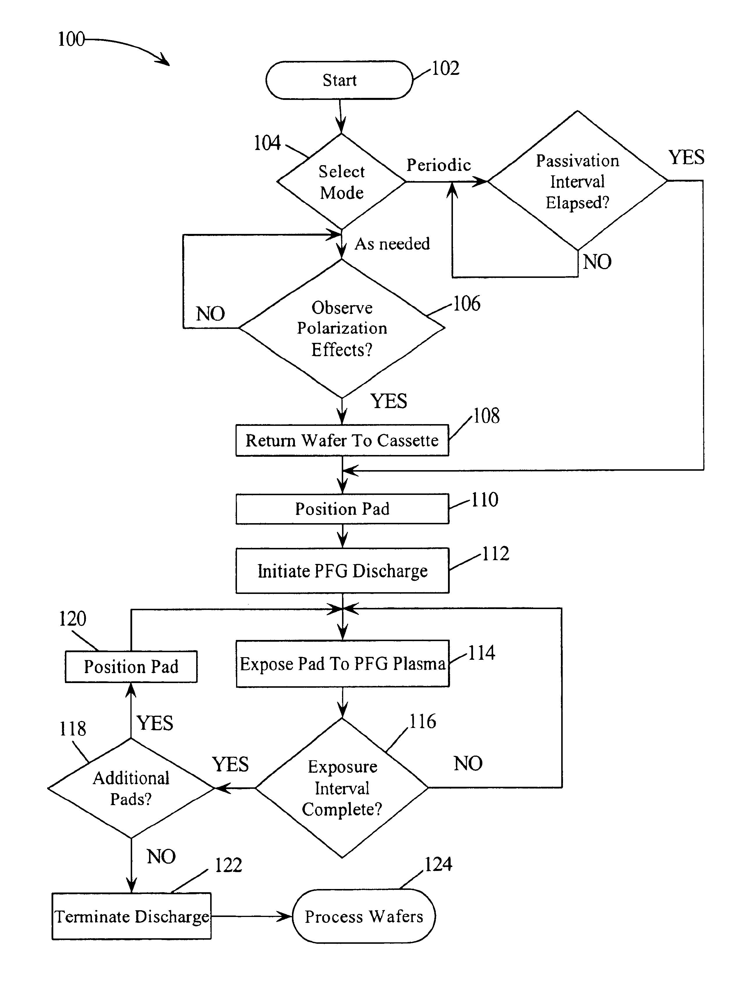
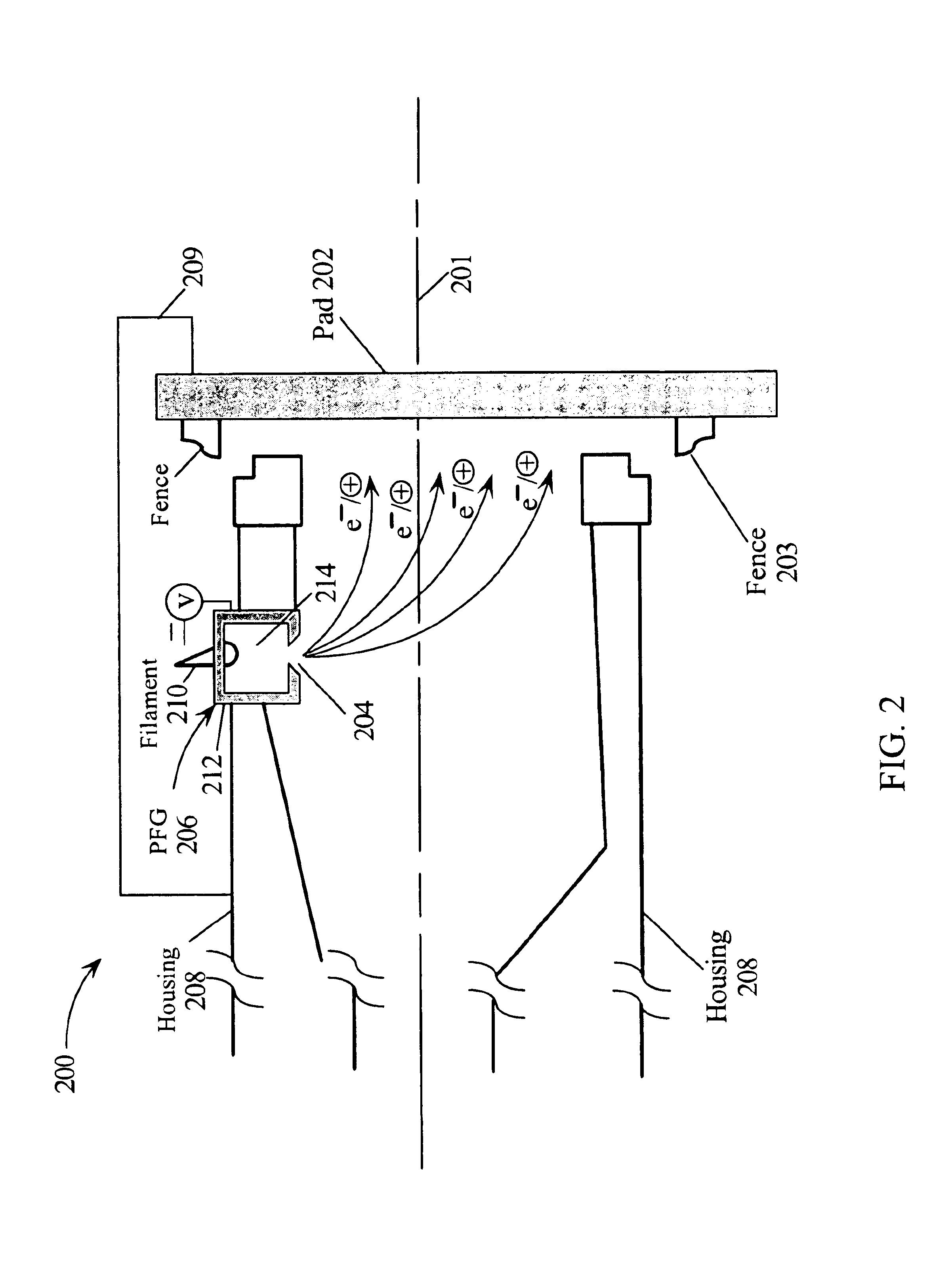
The present invention provides a mechanism for controlling a polarization of structures within a wafer fabrication tool. A high density plasma is generated within the vacuum volume of the tool, and the plasma is injected into the tool in the vicinity of structures susceptible to the buildup of polarization charges. Exposure of the structures to the plasma for a preselected interval of time relaxes the polarization.

In the following description, numerous specific details are set forth such as specific arc currents and voltages, and gas flow rates, etc., to provide a thorough understanding of the present invention. However, it will be obvious to those skilled in the art that the present invention may be practiced without such specific details. In other instances, well-known circuits have been shown in block diagram form in order not to obscure the present invention in unnecessary detail. For the most part, details concerning timing considerations and the like have been omitted in as mu...


PUM


Abstract

A method for electrostatic discharge depolarization is implemented. The buildup of charge on tool structures in fabrication tools for semiconductor processing may be expected to be of concern whenever high voltage is employed near the structure in a tool. The process herein includes selectively exposing the structure to a plasma for a selected time interval. The duration of the exposure time interval is sufficient to reduce the polarization of the structure whereby the forces due to the polarization do not interfere with the transport or movement of a wafer being processed.

Description

TECHNICAL FIELDThe present invention relates in general to semiconductor fabrication tools, and in particular, to the discharge of electrostatic charge buildup on the wafer pad or other structure in the process chambers of fabrication tools.BACKGROUND INFORMATIONElectrostatic discharge (ESD) control measures are typically employed in fabrication facilities for semiconductor devices. These control strategies are typically employed in the fabrication facilities external to the tools, however, currently, there are no generally applied protocols for neutralizing the buildup of electrical charges within the vacuum regions of the tools themselves.The buildup of charge on tool structures may be expected to be of concern whenever high voltage is employed near a wafer pad in a tool. For example, ion implants are used to introduce dopants into the underlying semiconductor material to produce the structural elements of the transistors constituting the integrated circuit device being fabricated...

Claims


Application Information

Patent Timeline
Patent Type & Authority Patents(United States)
IPC IPC(8): H01J61/00H01J37/02
CPCH01J37/026H01J2237/0041
Inventor ZHAO, ZHIYONGHENDRIX, DAVID
Owner ADVANCED MICRO DEVICES INC
Why Eureka
Try Eureka